Cascode amplifier structures including wide bandgap field effect transistor with field plates

a field effect transistor and amplifier structure technology, applied in the field of transistors, can solve the problems of low electron mobility, limiting performance, and degrading the high performance gain of si based hemt, and achieve the effect of efficient high power and high frequency signal amplification

Active Publication Date: 2006-10-24
CREE INC
View PDF10 Cites 73 Cited by
  • Summary
  • Abstract
  • Description
  • Claims
  • Application Information

AI Technical Summary

Benefits of technology

[0011]The present invention provides multiple staged amplifier circuits that take advantage of the desirable operating characteristics of non-field-plated transistors and field plated transistors to achieve efficient high power and high frequency signal amplification.

Problems solved by technology

One disadvantage of Si is that it has low electron mobility (approximately 1450 cm2 / V-s), which produces a high source resistance.
This resistance can degrade the Si based HEMT's high performance gain.
However, GaAs has a relatively small bandgap (1.42 eV at room temperature) and relatively small breakdown voltage, which prevents GaAs based HEMTs from providing high power at high frequencies.
Electron trapping and the resulting difference between DC and RF characteristics have been a limiting factor in the performance of GaN based transistors, such AlGaN / GaN HEMTs.
However, due to the high electric fields existing in these structures, charge trapping is still an issue.

Method used


Image

  • Cascode amplifier structures including wide bandgap field effect transistor with field plates
  • Cascode amplifier structures including wide bandgap field effect transistor with field plates
  • Cascode amplifier structures including wide bandgap field effect transistor with field plates

Examples


Embodiment Construction

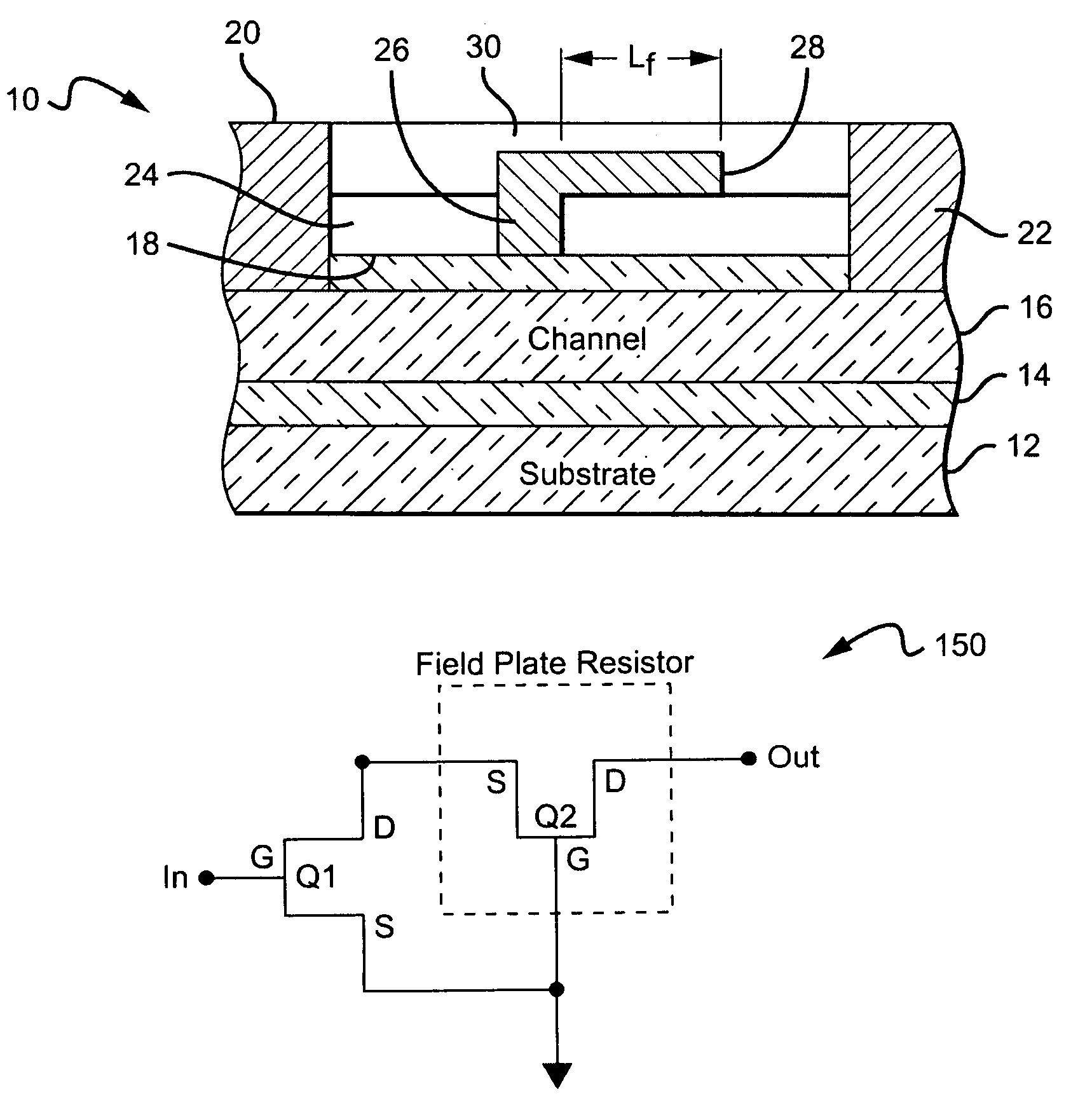
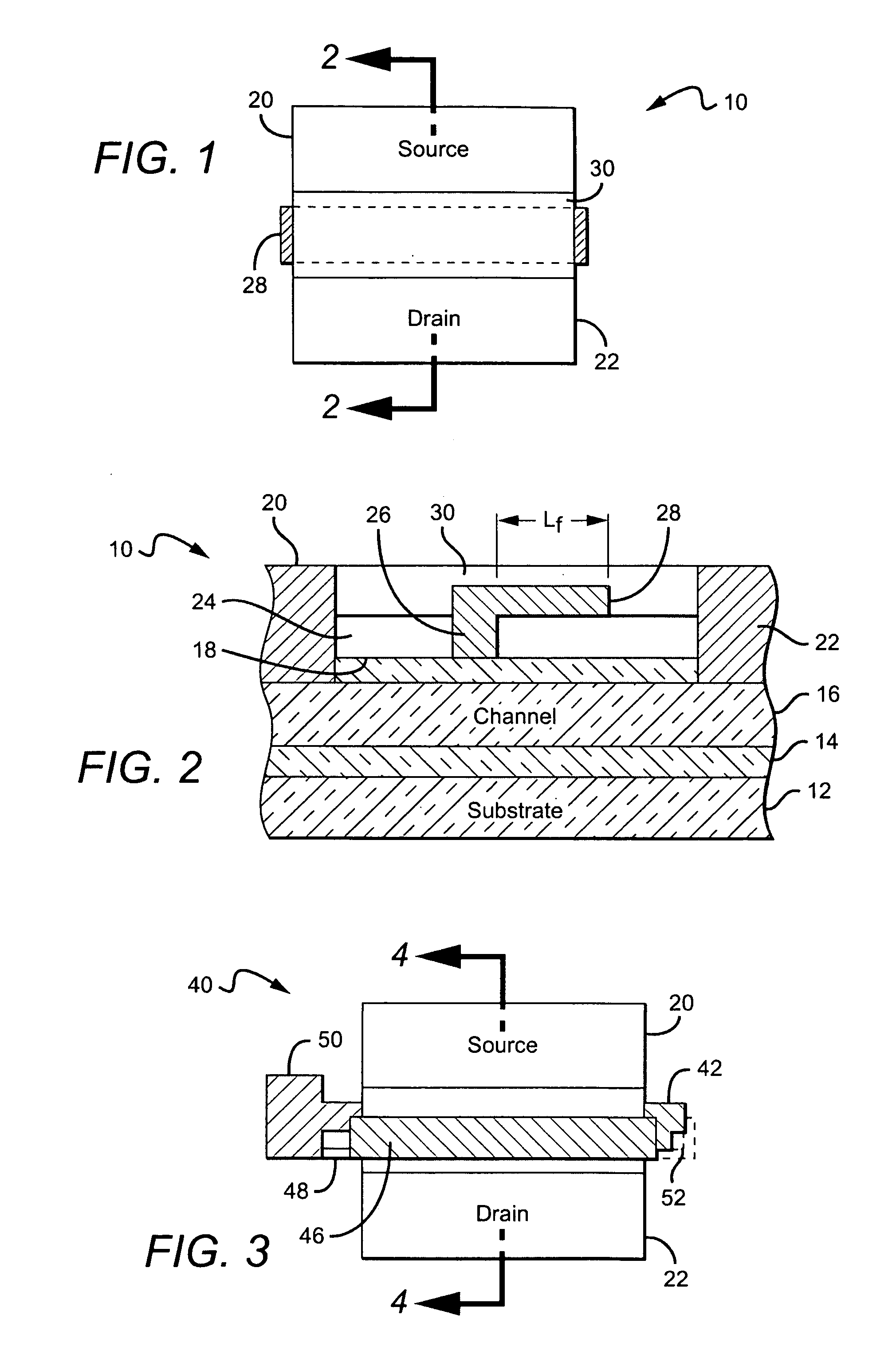
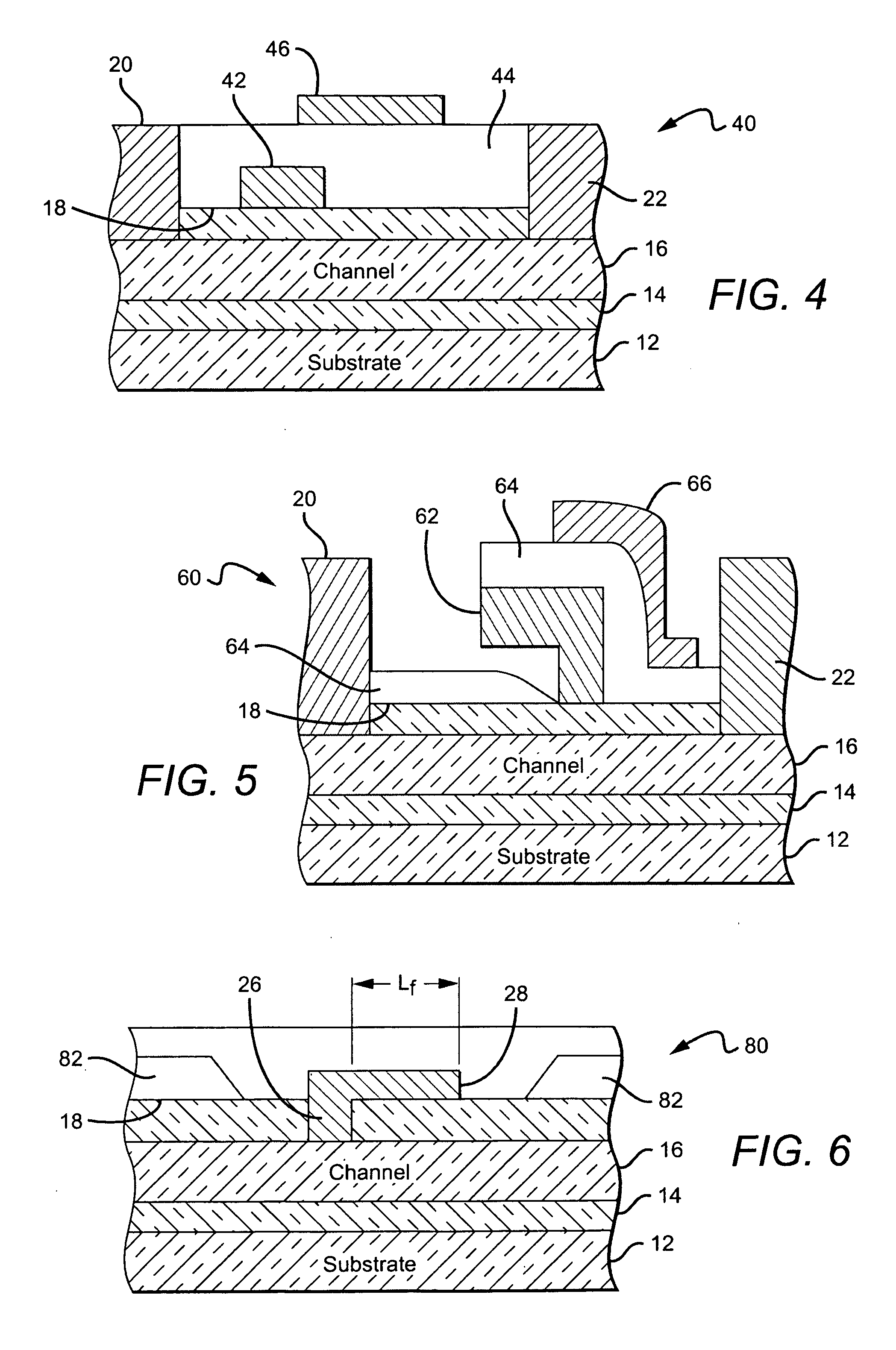
[0026]Multi-stage amplifier blocks according to the present invention combine the strengths of field plated and non-field-plated transistors. Field plated transistors can suffer from added capacitance (e.g. feedback) that can negatively impact overall performance. To address this an amplifier block is provided, preferably in a cascode arrangement, having at least two stages. One of the initial stages does not suffer from feedback capacitance and a downstream field plated stage is arranged in such a way that any added capacitance from a field plate only minimally impacts performance. Hence the multi-stage amplification block obtains the benefits of the field plate without detrimental impact on the overall gain of the amplifier block.

[0027]As more fully described below, one embodiment of an amplifier block according to the present invention comprises a 2-stage cascode arrangement including a first stage transistor connected in common source configuration and a second stage transistor ...


PUM


Abstract

A multi-stage amplifier circuit arranged to take advantage of the desirable characteristics of non-field-plate and field plate transistors when amplifying a signal. One embodiment of a multi-stage amplifier according to the present invention comprises a non-field-plate transistor and a field-plate transistor. The field-plate transistor has at least one field plate arranged to reduce the electric field strength within the field plate transistor during operation. The non-field plate transistor is connected to the field plate transistor, with the non-field-plate providing current gain and the field plate transistor providing voltage gain. In one embodiment the non-field-plate and field plate transistors are coupled together in a cascode arrangement.

Description

[0001]This application claims the benefit of provisional application Ser. No. 60 / 501,628 to Parikh et al., which was filed on Sep. 9, 2003.BACKGROUND OF THE INVENTION[0002]1. Field of the Invention[0003]The present invention relates to transistors and particularly to amplifier circuits utilizing field plated transistors.[0004]2. Description of the Related Art[0005]High electron mobility transistors (HEMTs) are a common type of solid state transistor that are regularly fabricated from semiconductor materials such as Silicon (Si) or Gallium Arsenide (GaAs). One disadvantage of Si is that it has low electron mobility (approximately 1450 cm2 / V-s), which produces a high source resistance. This resistance can degrade the Si based HEMT's high performance gain. [CRC Press, The Electrical Engineering Handbook, Second Edition, Dorf, p.994, (1997)][0006]GaAs based HEMTs have become the standard for signal amplification in civil and military radar, handset cellular, and satellite communications...

Claims


Application Information

Patent Timeline
Patent Type & Authority Patents(United States)
IPC IPC(8): H03F3/14H03F1/22H01L27/06H01L29/06H01L29/20H01L29/24H01L29/40H01L29/423H01L29/778H01L29/812
CPCH01L27/0605H01L29/402H01L29/42316H01L29/7787H01L29/812H01L29/1608H01L29/2003
Inventor MISHRA, UMESHPARIKH, PRIMITWU, YIFENG
Owner CREE INC
Why Eureka
Try Eureka