Process for producing group III nitride compound semiconductor

a technology of nitride and compound semiconductor, which is applied in the direction of polycrystalline material growth, crystal growth process, chemically reactive gas, etc., can solve the problems of no device but a semiconductor device low in mobility, device characteristic such as threshold current in ld and led cannot be improved, and no device but a semiconductor device can be formed

Inactive Publication Date: 2006-10-31
TOYODA GOSEI CO LTD
View PDF15 Cites 87 Cited by
  • Summary
  • Abstract
  • Description
  • Claims
  • Application Information

AI Technical Summary

Benefits of technology

[0009]Although there has been already proposed a technique in which a difference in level, a surface roughness, or the like is provided on a surface of a substrate so that a Group III nitride compound semiconductor can be epitaxially laterally overgrown, a method particularly remarkably effective in producing a Group III nitride compound semiconductor can be found by the subsequent examination when a substrate, a substrate surface and a buffer layer and methods for forming these are combined as follows. According to the invention, modification of the surface of the sapphire substrate can be achieved by etching in a very short time without necessity of forming a difference of 0.1 μm in level. According to the invention, epitaxial growth of the Group III nitride compound semiconductor can be made continuously from vertical and lateral epitaxial growth on the AlN buffer layer. Because the AlN buffer layer is formed by means of reactive sputtering, the growth of the Group III nitride compound semiconductor can be made by integrated production after the substrate is mounted in a Group III nitride compound semiconductor growth apparatus. Accordingly, a Group III nitride compound semiconductor layer suppressed in terms of threading dislocation can be formed by a smaller number of steps as a whole.

Problems solved by technology

For this reason, there is a problem that device characteristic becomes poor.
There is a problem that dislocation of about 109 cm−2 propagates in the Group III nitride compound semiconductor.
For example, in the case of a light-emitting device, there is therefore a problem that device characteristic such as threshold current in LD, device life in LD and LED, etc. cannot be improved.
Also in the case of another semiconductor device, no device but a semiconductor device low in mobility can be formed because electrons are scattered by defects.
These problems occur also in the case where another substrate is used.
As a result, when separation into devices is performed in an after-process, peeling, cracking or chipping occurs in the portion where the space is formed.

Method used


Image

  • Process for producing group III nitride compound semiconductor
  • Process for producing group III nitride compound semiconductor
  • Process for producing group III nitride compound semiconductor

Examples


embodiment

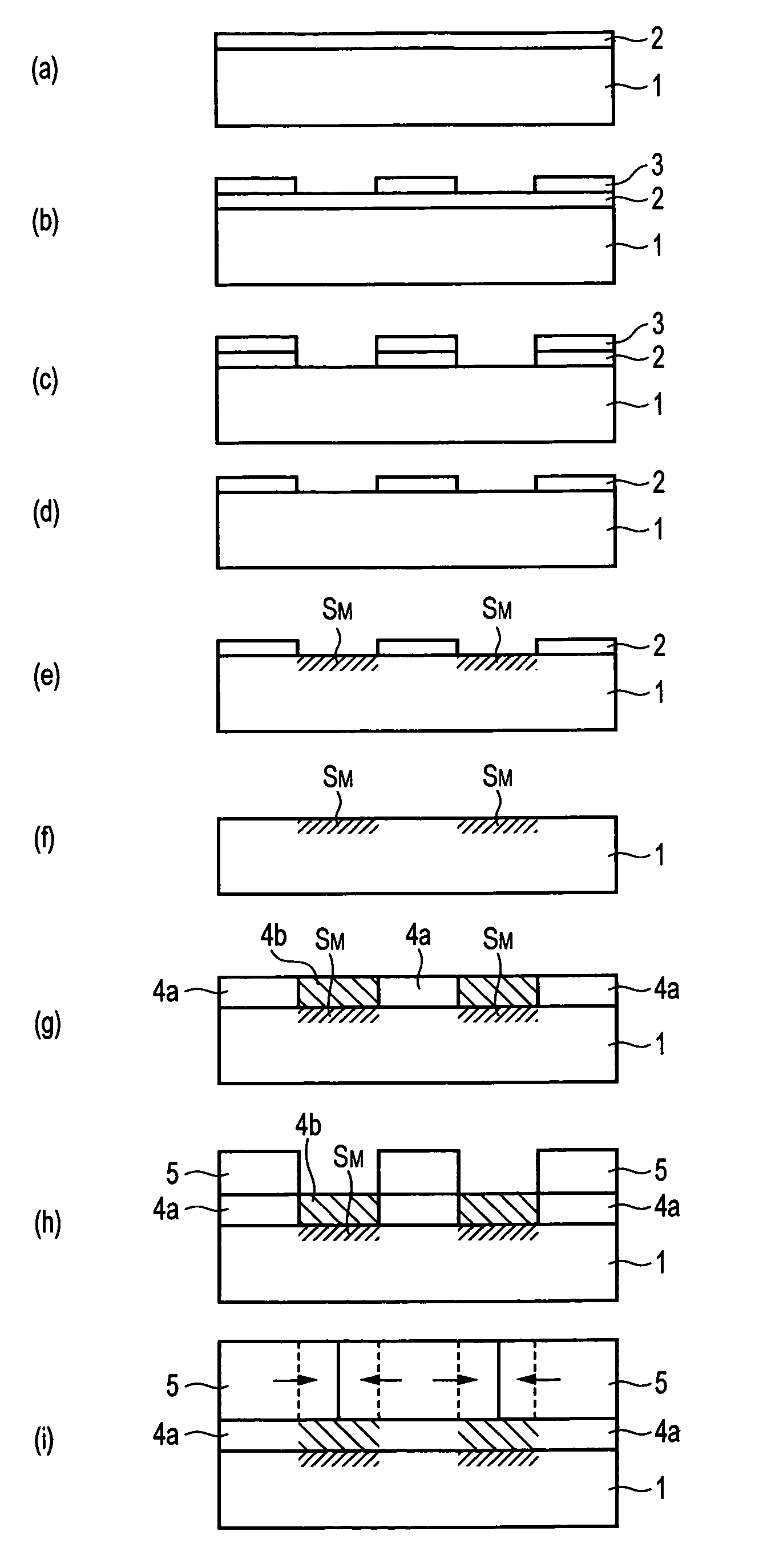
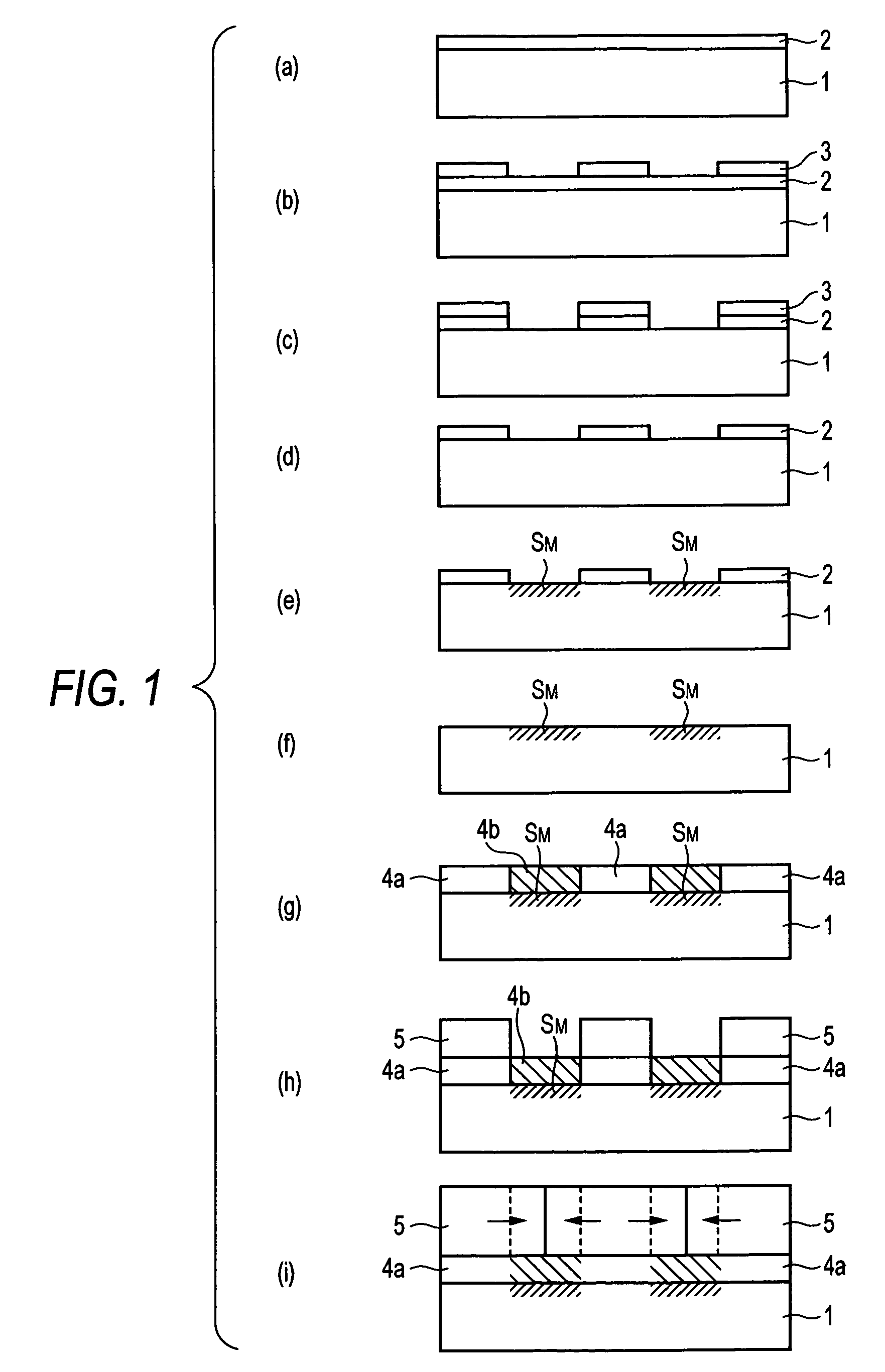
[0013]In the condition that a face A of a mono-crystalline sapphire substrate 1 cleaned by organic cleaning was used as a principal surface, that is, as a crystal growth surface, a 50-nm thick Ni film 2 was deposited on the mono-crystalline sapphire substrate 1 by means of vapor deposition (FIG. 1(a)) Then, the Ni film 2 was coated with a photo resist 3 and the photo resist 3 was patterned in the form of stripes on the face A, that is, on the flat surface by photolithography. The patterning was made in a direction perpendicular to the axis c of the sapphire substrate 1 so that both the width of each stripe of the photo resist 3 and the distance between adjacent stripes of the photo resist 3 were 5 μm (FIG. 1(b)).

[0014]Then, the Ni film 2 was removed with acid from portions where the photo resist 3 had been already removed (FIG. 1(c)). Then, the photo resist 3 was removed by organic cleaning. In this manner, an etching mask of the Ni film 2 was formed to have 5 μm-wide and 5 μm-dista...


PUM

PropertyMeasurementUnit
widthaaaaaaaaaa
thicknessaaaaaaaaaa
temperatureaaaaaaaaaa

Abstract

A method including the steps of: modifying at least one part of a sapphire substrate by dry etching to thereby form any one of a dot shape, a stripe shape, a lattice shape, etc. as an island shape on the sapphire substrate; forming an AlN buffer layer on the sapphire substrate; and epitaxially growing a desired Group III nitride compound semiconductor vertically and laterally so that the AlN layer formed on a modified portion of the surface of the sapphire substrate is covered with the desirably Group III nitride compound semiconductor without any gap while the AlN layer formed on a non-modified portion of the surface of the sapphire substrate is used as a seed, wherein the AlN buffer layer is formed by means of reactive sputtering with Al as a target in an nitrogen atmosphere.

Description

TECHNICAL FIELD[0001]The present invention relates to a method for producing a Group III nitride compound semiconductor. Particularly it relates to a method for producing a Group III nitride compound semiconductor by using epitaxial lateral overgrowth (ELO), a Group III nitride compound semiconductor device and a Group III nitride compound semiconductor substrate. Incidentally, the Group III nitride compound semiconductor may be represented by the general formula AlxGayIn1-x-yN (0≦x≦1, 0≦y≦1, 0≦x+y≦1) which includes: binary compounds such as AlN, GaN and InN; ternary compounds such as AlxGa1-xN, AlxIn1-xN and GaxIn1-xN (0x<1 each); and quaternary compounds such as AlxGayIn1-x-yN (0<x<1, 0<y<1, 0<x+y<1). In this description, the expression “Group III nitride compound semiconductor” simply implies a Group III nitride compound semiconductor doped with impurities to change the conduction type to a p type or an n type if no further notice is given particularly.BACKGR...

Claims


Application Information

Patent Timeline
Patent Type & Authority Patents(United States)
IPC IPC(8): C23F1/00C30B29/38C30B25/02C30B25/18C30B29/40H01L21/20H01L21/205H01L33/12H01L33/16H01L33/32
CPCC30B25/02C30B25/18C30B29/40C30B29/403H01L21/0242H01L21/02458H01L21/0254H01L21/0262H01L21/02631H01L21/02639H01L21/02647
Inventor NISHIJIMA, KAZUKISENDA, MASANOBUCHIYO, TOSHIAKIITO, JUNSHIBATA, NAOKIHAYASHI, TOSHIMASA
Owner TOYODA GOSEI CO LTD
Why Eureka
Try Eureka