Manufacturing method of fin-type field effect transistor

a field effect transistor and manufacturing method technology, applied in the direction of basic electric elements, electrical apparatus, semiconductor devices, etc., can solve the problems of inability to achieve desired values, and inability to improve the dielectric constant by using silicon oxynitride films

Inactive Publication Date: 2008-07-17
TOKYO ELECTRON LTD
View PDF6 Cites 192 Cited by
  • Summary
  • Abstract
  • Description
  • Claims
  • Application Information

AI Technical Summary

Benefits of technology

[0025]In view of the foregoing, the present invention provides a method for manufacturing a fin-type field effect transistor simply and securely by using a SOI wafer, capable of suppressing an undercut formation at a base portion of a fin, and even c...

Problems solved by technology

Though germanium, gallium-arsenic, and so forth are available as semiconductor materials having high carrier mobility, a practical use of them is yet to be accomplished for the reason that their use addresses thermal safety issues or renders it difficult to form a fine semiconductor/insulator interface, and so forth.
However, improvement of the dielectric constant by the use of the silicon oxynitride film is deemed to have a limit, and a high-k insulating film having a higher dielectric constant is expected to be used as a promising next-generation gate insulating film.
However, as reported from recent researches, in the event that a poly-Si or metal gate electrode is used on the gate insulating film made of the HfO2 or the Hf-silicate, a work function of the gate electrode varies 2)(Fermi level peening), causing a problem that a threshold voltage cannot be regulated at a desired value.
Further, it is also known that carrier mobility deteriorates due to the influence of stationary charges in the insulating film, dipoles generated in an interface layer between the gate electrode and the insulating film, remote phonon scattering, and the like.
However, the increase of the doping concentration would cause an increase o...

Method used


Image

  • Manufacturing method of fin-type field effect transistor
  • Manufacturing method of fin-type field effect transistor
  • Manufacturing method of fin-type field effect transistor

Examples


Embodiment Construction

[0041]Hereinafter, an embodiment of the present invention will be described.

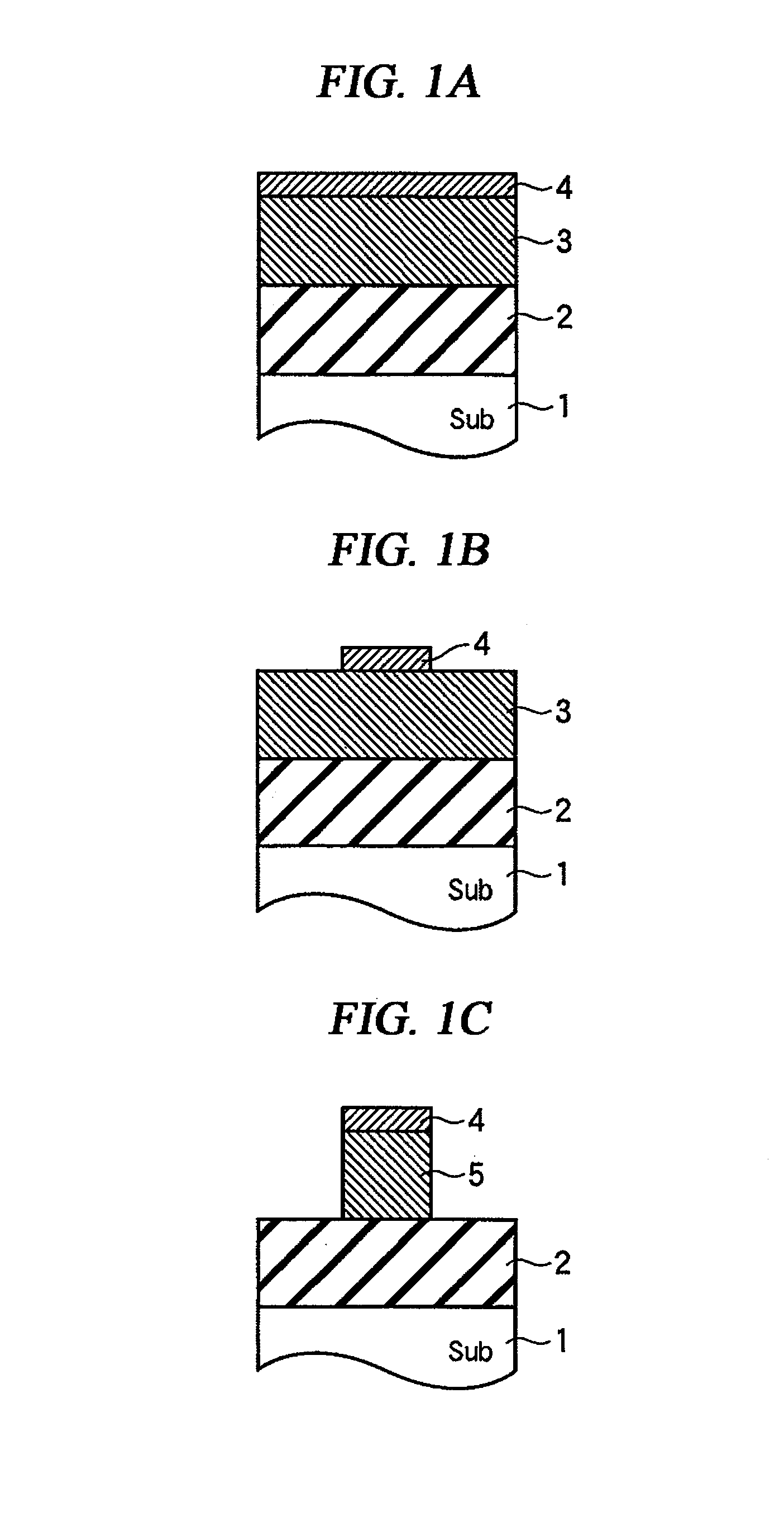
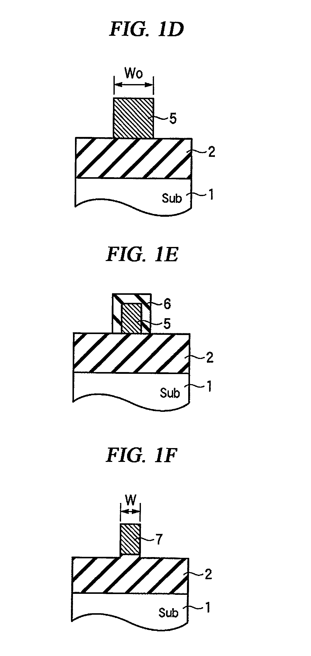
[0042]FIGS. 1A to 1F provide cross sectional views to describe a process sequence of a manufacturing method for a fin-type field effect transistor in accordance with an embodiment of the present invention. The manufacturing method in accordance with the embodiment is performed by using a SOI (Silicon On Insulator) wafer, and the method involves the steps of forming a protrusion by dry etching, forming a sacrificial oxide film on the protrusion, and removing the sacrificial oxide film by wet etching.

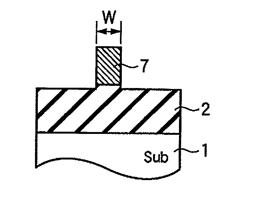
[0043]In the embodiment, a SOI wafer having a multilayer structure shown in FIG. 1A is first prepared. The SOI wafer includes a silicon substrate 1 made of single crystalline silicon, a buried oxide layer 2, a single crystalline silicon layer 3 and a hard mask 4 that are laminated in sequence.

[0044]The buried oxide layer 2 is made of SiO2 formed by a thermal oxidation method. Here, a thermal oxidation temperature ...


PUM


Abstract

A method for manufacturing a fin-type field effect transistor simply and securely by using a SOI (Silicon On Insulator) wafer, capable of suppressing an undercut formation, is disclosed. The method includes forming a fin-shaped protrusion by selectively dry-etching a single crystalline silicon layer until an underlying buried oxide layer is exposed; forming a sacrificial oxide film by oxidizing a surface of the protrusion including a damage inflicted thereon; and forming a fin having a clean surface by removing the sacrificial oxide film by etching, wherein an etching rate r1 of the sacrificial oxide film is higher than an etching rate r2 of the buried oxide layer during the etching.

Description

FIELD OF THE INVENTION[0001]The present invention relates to a method for manufacturing a fin-type field effect transistor by using a SOI (Silicon On Insulator) wafer.BACKGROUND OF THE INVENTION[0002]Recent primary concern for the development of a very large scale integration (VLSI) circuit is to increase a driving current of a metal oxide semiconductor field effect transistor (MOSFET) while reducing power consumption thereof. To meet such requirement, it has been investigated to use a material having higher carrier mobility than silicon as a channel material. Though germanium, gallium-arsenic, and so forth are available as semiconductor materials having high carrier mobility, a practical use of them is yet to be accomplished for the reason that their use addresses thermal safety issues or renders it difficult to form a fine semiconductor / insulator interface, and so forth. Accordingly, it has been attempted to increase the driving current by way of miniaturizing the MOSFET by using ...

Claims


Application Information

Patent Timeline
IPC IPC(8): H01L21/82
CPCH01L29/66818H01L21/18H01L21/302
Inventor NAKABAYASHI, HAJIMESUGAWARA, TAKUYAKOBAYASHI, TAKASHIKITAGAWA, JUNICHITANAKA, YOSHITSUGU
Owner TOKYO ELECTRON LTD
Why Eureka
Try Eureka