High-temperature selective dry etch having reduced post-etch solid residue

a dry etching and high temperature selective technology, applied in the field of manufacturing technology, can solve the problems of slow etching, affecting the etching speed of the self-limiting process, and etching silicon too quickly, and achieve the effect of reducing the solid residue on the etched surface and high dielectric film temperatur

Active Publication Date: 2013-07-02
APPLIED MATERIALS INC
View PDF10 Cites 177 Cited by
  • Summary
  • Abstract
  • Description
  • Claims
  • Application Information

AI Technical Summary

Benefits of technology

[0007]Methods of dry etching silicon-containing dielectric films are described. The methods include maintaining a relatively high temperature of the dielectric films while etching in order to achieve reduced solid residue on the etched surface. Partially or completely avoiding the accumulation of solid residue increases the etch rate.

Problems solved by technology

Siconi™ etches have been developed which are largely conformal and selective towards silicon oxide layers while not readily etching silicon regardless of whether the silicon is amorphous, crystalline or polycrystalline.
These self-limiting processes etch more slowly as the solid by-products accumulate and the progress would eventually stop.

Method used


Image

  • High-temperature selective dry etch having reduced post-etch solid residue
  • High-temperature selective dry etch having reduced post-etch solid residue
  • High-temperature selective dry etch having reduced post-etch solid residue

Examples


Embodiment Construction

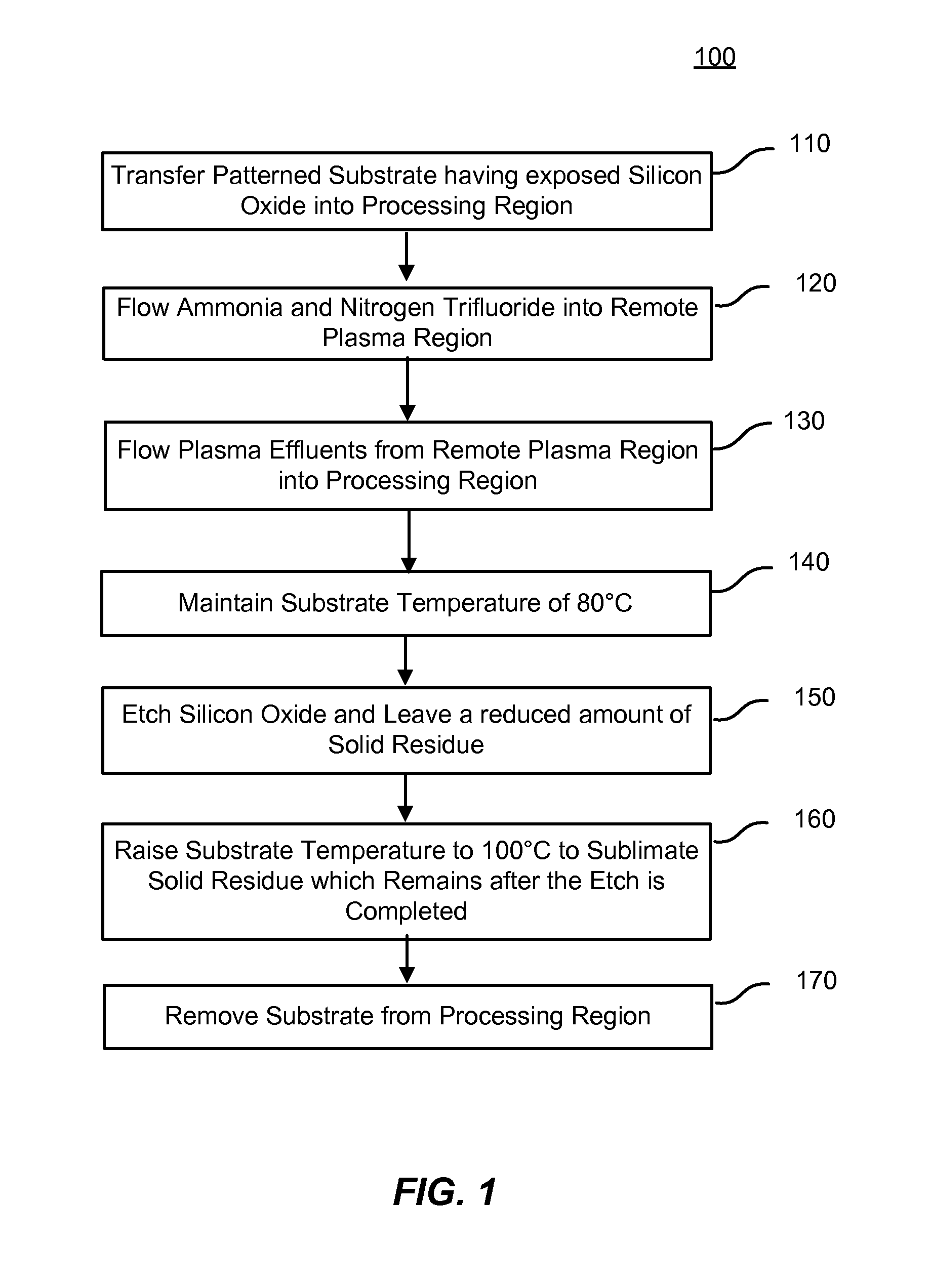
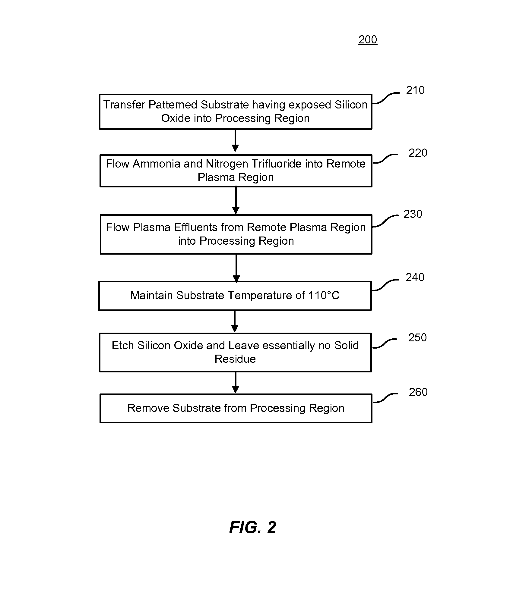
[0015]Methods of dry etching silicon-containing dielectric films are described. The methods include maintaining a relatively high temperature of the dielectric films while etching in order to achieve reduced solid residue on the etched surface. Partially or completely avoiding the accumulation of solid residue increases the etch rate.

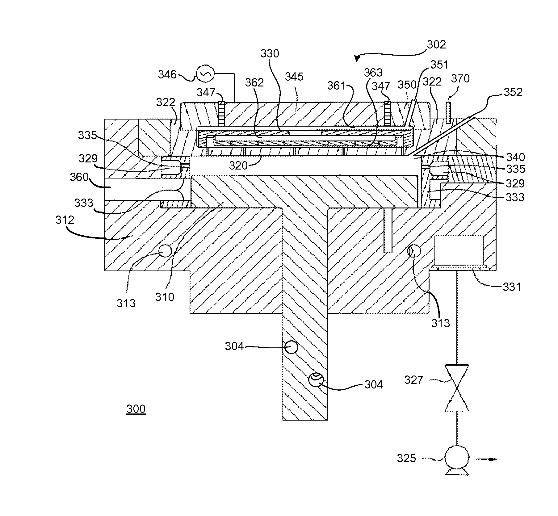
[0016]Siconi™ etch processes have used a hydrogen source of ammonia (NH3) and a fluorine source of nitrogen trifluoride (NF3) which together flow into a remote plasma system (RPS). The plasma effluents created therein are flowed into a substrate processing region. Previously, substrate temperatures have been kept relatively low during the etching operation in order to remove a given amount of material during each etch-sublimation cycle. While performing a Siconi™ etch, solid by-products are formed at nucleation sites distributed across a substrate surface. The solid by-products grow larger as material is consumed from the top layer of the substrate. As ...


PUM

PropertyMeasurementUnit
processing temperatureaaaaaaaaaa
temperatureaaaaaaaaaa

Abstract

Methods of dry etching silicon-containing dielectric films are described. The methods include maintaining a relatively high temperature of the dielectric films while etching in order to achieve reduced solid residue on the etched surface. Partially or completely avoiding the accumulation of solid residue increases the etch rate.

Description

CROSS-REFERENCES TO RELATED APPLICATIONS[0001]This application claims the benefit of U.S. Provisional Patent Application No. 61 / 330,097 filed Apr. 30, 2010, and titled “CONCURRENT SUBLIMATION SICONI ETCH,” which is incorporated herein by reference for all purposes.FIELD OF THE INVENTION[0002]This application relates to manufacturing technology solutions involving equipment, processes, and materials used in the deposition, patterning, and treatment of thin-films and coatings, with representative examples including (but not limited to) applications involving: semiconductor and dielectric materials and devices, silicon-based wafers and flat panel displays (such as TFTs).BACKGROUND OF THE INVENTION[0003]Integrated circuits are made possible by processes which produce intricately patterned material layers on substrate surfaces. Producing patterned material on a substrate requires controlled methods for removal of exposed material. Chemical etching is used for a variety of purposes includ...

Claims


Application Information

Patent Timeline
Patent Type & Authority Patents(United States)
IPC IPC(8): B44C1/22
CPCH01L21/31116H01J37/32357
Inventor THADANI, KIRAN V.TANG, JINGINGLE, NITINYANG, DONGQING
Owner APPLIED MATERIALS INC
Why Eureka
Try Eureka