
Semiconductor device with floating block

a floating block and semiconductor technology, applied in the direction of identification means, instruments, applications, etc., can solve the problems of difficult to ensure the circuit operation of the semiconductor device, the risk of the control circuit being damaged, and the output mos transistor b>36/b>, etc., to achieve high reference voltage accuracy, stable operation of the integrated signal processing circuit, and good stability

Inactive Publication Date: 2006-10-31
COLLABO INNOVATIONS INC
View PDF1 Cites 7 Cited by
  • Summary
  • Abstract
  • Description
  • Claims
  • Application Information

AI Technical Summary

Benefits of technology

"The present invention relates to a semiconductor device that includes a high-potential power source terminal, a floating block, a MOS transistor, bipolar transistors, resistors, and a differential amplifier. The device allows for the formation of transistor active regions in the floating block by using commonly connected collectors and bases. The device also includes a comparator for detecting power source fluctuations and ensuring stable operation of the integrated signal processing circuit. Additionally, the device prevents breakdown caused by abnormal operation during power source voltage decrease and rising ambient temperature. The technical effects of the invention include improved accuracy of reference voltage, stable operation of the integrated signal processing circuit, and prevention of breakdown."

Problems solved by technology

For this reason, the circuit operates in a state in which the power source voltage of the control circuit fluctuates, and if the surge voltage is superimposed on the power source voltage, there is a risk of the control circuit being damaged.
Moreover, there is also a risk of the output MOS transistors 36, 37 being damaged.
As a result, the detection sensitivity of the protection circuit 7 is different for each semiconductor device, or the detection sensitivity changes depending on the ambient temperature, and the circuit operation of the semiconductor device is difficult to ensure.
As a result, the spread cannot be decreased to a level of linear circuits composed of bipolar transistors.
A problem associated with bipolar transistors with a high voltage resistance is that a guard ring has to be formed inside the island region forming the transistor, and the unit shape becomes larger than that of the usual bipolar transistor.
As described hereinabove, when a reference voltage circuit 20 with a simple circuit configuration shown in FIG. 5 was employed, the problem was that the production spread of the resistor 21 or MOS transistor 22 was large, in particular, the spread in the threshold voltage Vt of the MOS transistor 22 degraded the detection accuracy of the protection circuit 7 and sufficient electric characteristics of the semiconductor device could not be guaranteed.
For all that, in the case of forming a circuit by using a large number of MOS transistors, a sufficient accuracy of relative values of the MOS transistors cannot be obtained and a circuit design ensuring absolute values of detection accuracy of the protection circuit 7 is difficult to provide.
However, the problem is that bipolar transistors with a high voltage resistance characteristic are required for integrating the sustain drive 102, and configuring the circuit by using bipolar transistors with a high voltage resistance that comprise guard rings degrades the degree of integration of the semiconductor device.

Method used


Image

  • Semiconductor device with floating block
  • Semiconductor device with floating block
  • Semiconductor device with floating block

Examples


embodiment 1

(Embodiment 1)

[0056]FIG. 1 and FIG. 2 illustrate Embodiment 1 of the present invention.

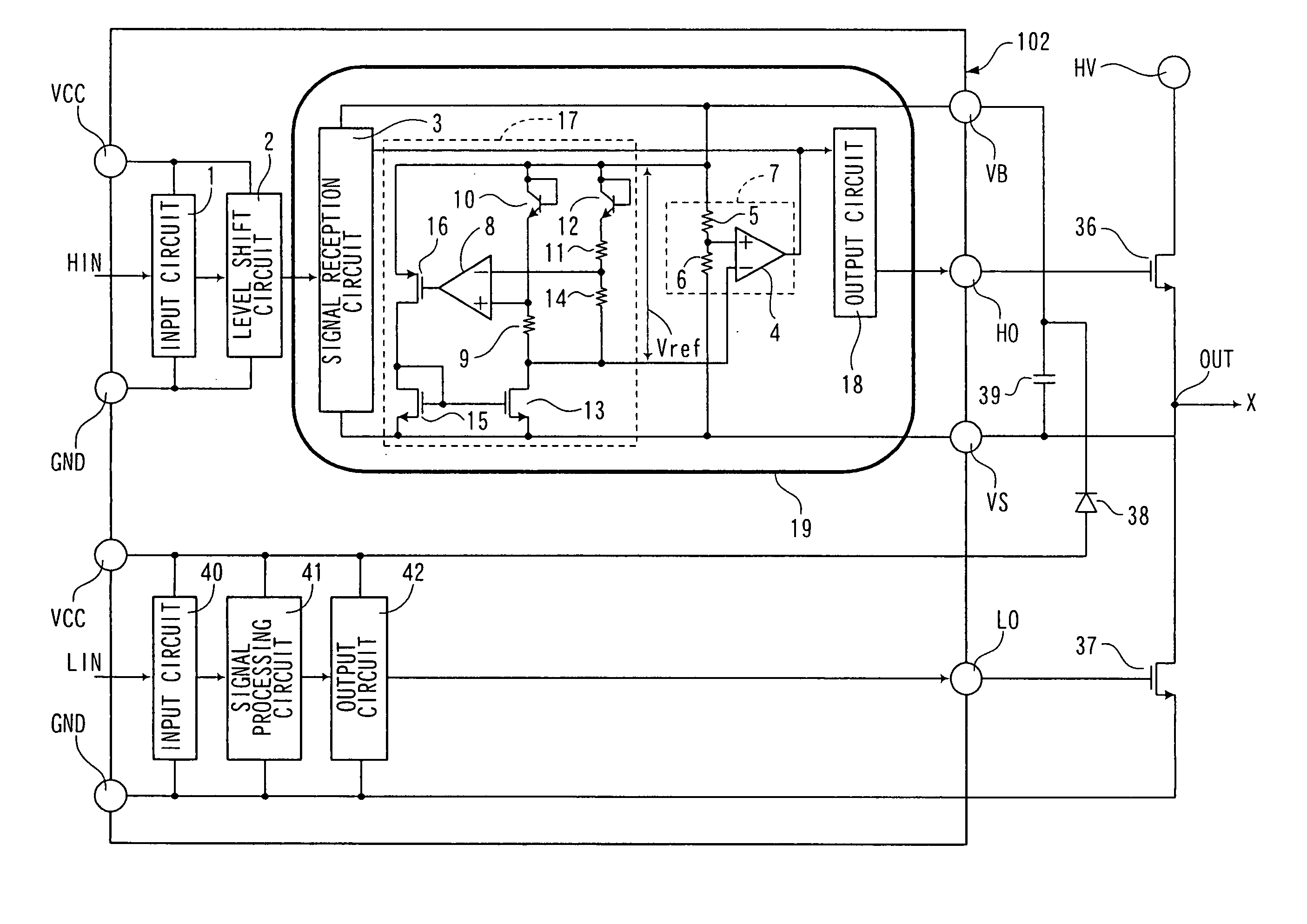
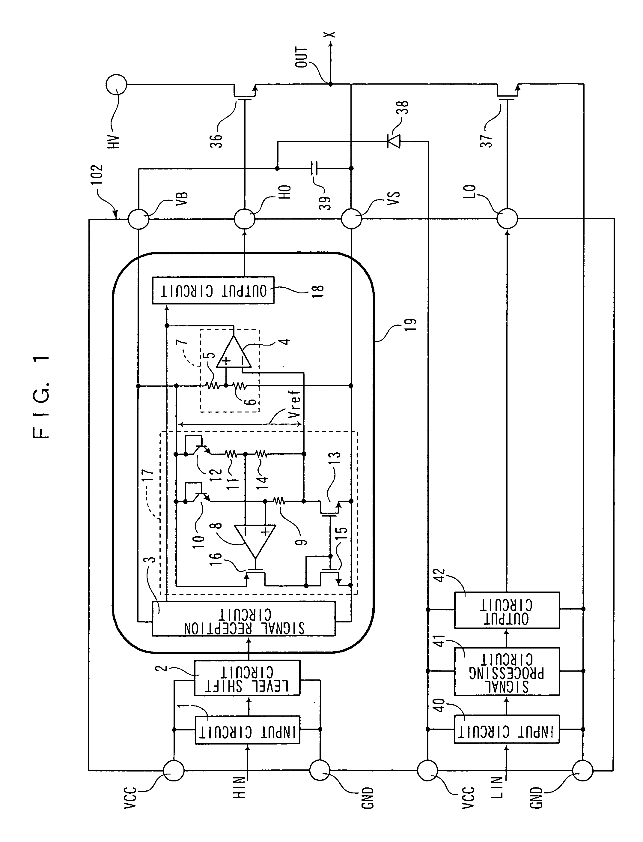
[0057]FIG. 1 shows a semiconductor device for PDP signal processing that uses a sustain driver 102 comprising a boot strap circuit.

[0058]In the sustain driver shown in FIG. 1, an input circuit 1 and a level shift circuit 2 operate by using a power source voltage applied between a power source terminal VCC and a ground terminal GND.

[0059]A floating block 19 with a high voltage resistance is an island region of an N-type semiconductor configured inside a semiconductor substrate. A high-potential power source terminal. VB is connected to this island region, the island potential is biased by the voltage applied to the high-potential power source terminal and varies from a low potential (about 20 V) to a high potential (about 400 V). Further, a low-potential power source terminal VS serves for a signal processing circuit integrated inside the floating block 19 with a high voltage resistance.

[0060]A sig...

embodiment 2

(Embodiment 2)

[0077]Described hereinbelow is a semiconductor device comprising a protection circuit operating when the power source voltage drops.

[0078]The circuit of Embodiment 2 has a configuration almost identical to that shown in FIG. 1 (Embodiment 1), wherein the high-potential power source terminal voltage VB divided by the resistors 5, 6 is applied to the inverted input terminal (−) of the comparator 4 and the drain voltage of the MOS transistor 13 is applied to the non-inverted input terminal (+). As a result, when the voltage between the terminals of the resistor 5 becomes less than the reference voltage Vref, the comparator 4 can terminate the output of signal (Vout) processing circuit (output circuit 18) integrated in the floating block 19. In this case, it functions as a protection circuit for terminating the operation of the signal processing circuit before the power source voltage drops and becomes insufficient. However, the operation point of the power source voltage ...

embodiment 3

(Embodiment 3)

[0080]A semiconductor device comprising a circuit protecting against heating will be described with reference to FIG. 3.

[0081]FIG. 3 shows the circuit configuration of Embodiment 3 of the present invention. The explanation of the signal reception circuit 3, reference voltage circuit 17, protection circuit 7 for protection against over-voltage, and output circuit 18 will be omitted.

[0082]The above-mentioned reference voltage Vref is resistance divided by the serial circuit of a resistor 33 and a resistor 34 connected to the reference voltage circuit 17, and the prescribed voltage corresponding to the operation point at the detected temperature is set. The collector and base of a bipolar transistor 31 are connected to a high-potential power source terminal VB and the emitter of the bipolar transistor 31 is connected to one terminal of a constant-current source 32 to supply a constant current. Further, the inverted input terminal (−) of a comparator 30 is connected to the...


PUM


Abstract

A band gap circuit using NPN transistors (10, 12) having collectors connected to a power source voltage is employed, and transistor active regions of the NPN transistors (10, 12) and semiconductor elements constituting other signal processing circuits are integrated in the same floating block (19) with high voltage resistance. As a result, a reference voltage circuit used in the signal processing circuit can be integrated in a compact manner.

Description

BACKGROUND OF THE INVENTION[0001]1. Field of the Invention[0002]The present invention relates to a sustain driver for applying a discharge sustain pulse voltage to electrodes of a plasma display panel.[0003]2. Description of the Related Art[0004]Plasma display devices, as shown in FIG. 4, comprise a PDP 101, a sustain driver 102, a scan driver 103, a data driver 104, and a panel control unit 105.[0005]In the PDP 101 with a three-electrode surface discharge structure, address electrodes A are arranged in the vertical direction of the panel on a rear-surface substrate, and sustain electrodes X and scanning electrodes Y are arranged alternately in the transverse direction of the panel on the rear-surface substrate.[0006]The sustain electrodes X are connected to each other and have substantially the same potential. The potential of the address electrodes A and scanning electrodes Y can be varied by one electrode at a time with the data driver 104 and scan driver 103.[0007]Discharge cell...

Claims


Application Information

Patent Timeline
Patent Type & Authority Patents(United States)
IPC IPC(8): H03F1/00H01L21/331G05F3/30G09F9/313H01J17/49H01L21/822H01L21/8222H01L21/8234H01L21/8248H01L21/8249H01L23/58H01L27/04H01L27/06H01L29/06H01L29/73H01L29/732
CPCG05F3/30H01L27/0635H01L29/0692H01L29/73H01L29/0619A23V2002/00A23V2300/16A23V2300/24A23L13/67A23P30/20
Inventor INAO, MASASHIMATSUNAGA, HIROKI
Owner COLLABO INNOVATIONS INC
Learn More