
Patsnap Eureka
For R&D, Patsnap Eureka makes reading and utilizing patents & technical documents easy.
Patsnap Eureka AIR
Designed for self-driven R&D workflows. Generate viable solutions, solve complex R&D challenges, empower your innovation with AI.

Patsnap Eureka Materials
Designed for material experts only. Revolutionize your material R&D, from search, analyze, to developing new materials.

TechResearch
Generate reliable direction feasibility study reports for your R&D in just a few steps.

TechSeek
Discover and master advanced knowledge NOW. Basics, ideas, possibilities, all at once.

TechMind
As an expert in R&D Theories, TechMind can generates customized viable solutions instantly.

TechRisk
Analyze your overall solution with one click, know your potential R&D risks in advance.

TechMonitor
Get weekly tech updates, stay abreast of the latest tech innovations and key insights.
Radiation detector and radiation detecting element
- Summary
- Abstract
- Description
- Claims
- Application Information
AI Technical Summary
Benefits of technology
Problems solved by technology
Method used
Image

Examples
Embodiment Construction
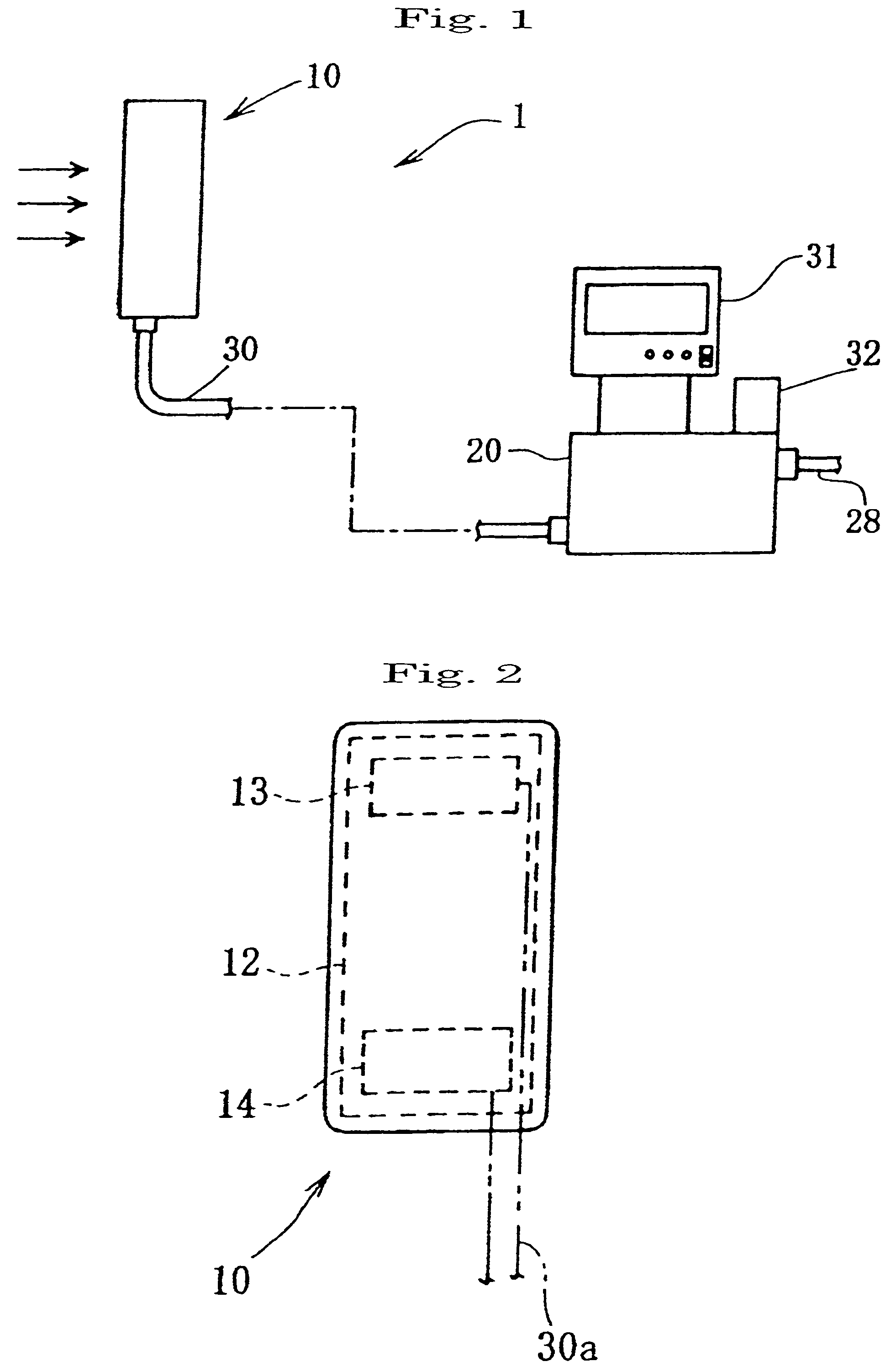
[0027]A description is now given of the preferred embodiments of the present invention. As shown in FIG. 1, a radiation detector 1 of this preferred embodiment detects and measures the intensity of γ-rays constituting ionizing radiation. The radiation detector 1 includes a radiation detection element 10 for detecting radiation, a control unit 20, a coaxial cable 30, a display unit 31, and an alarm 32.
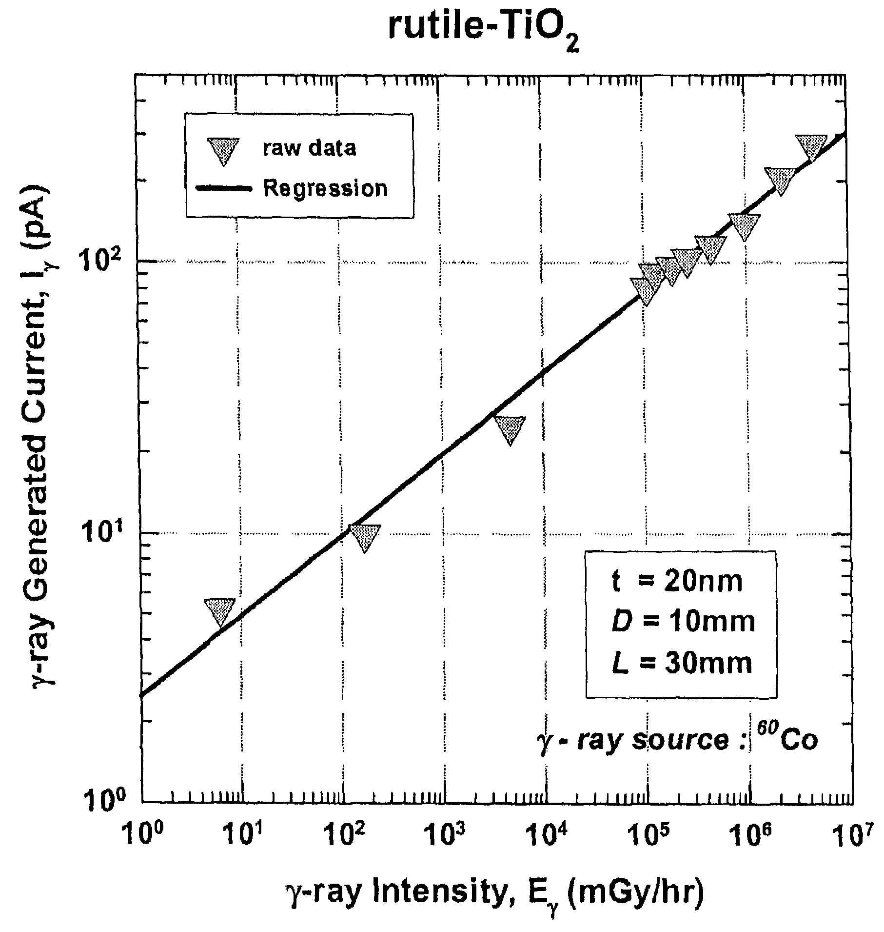
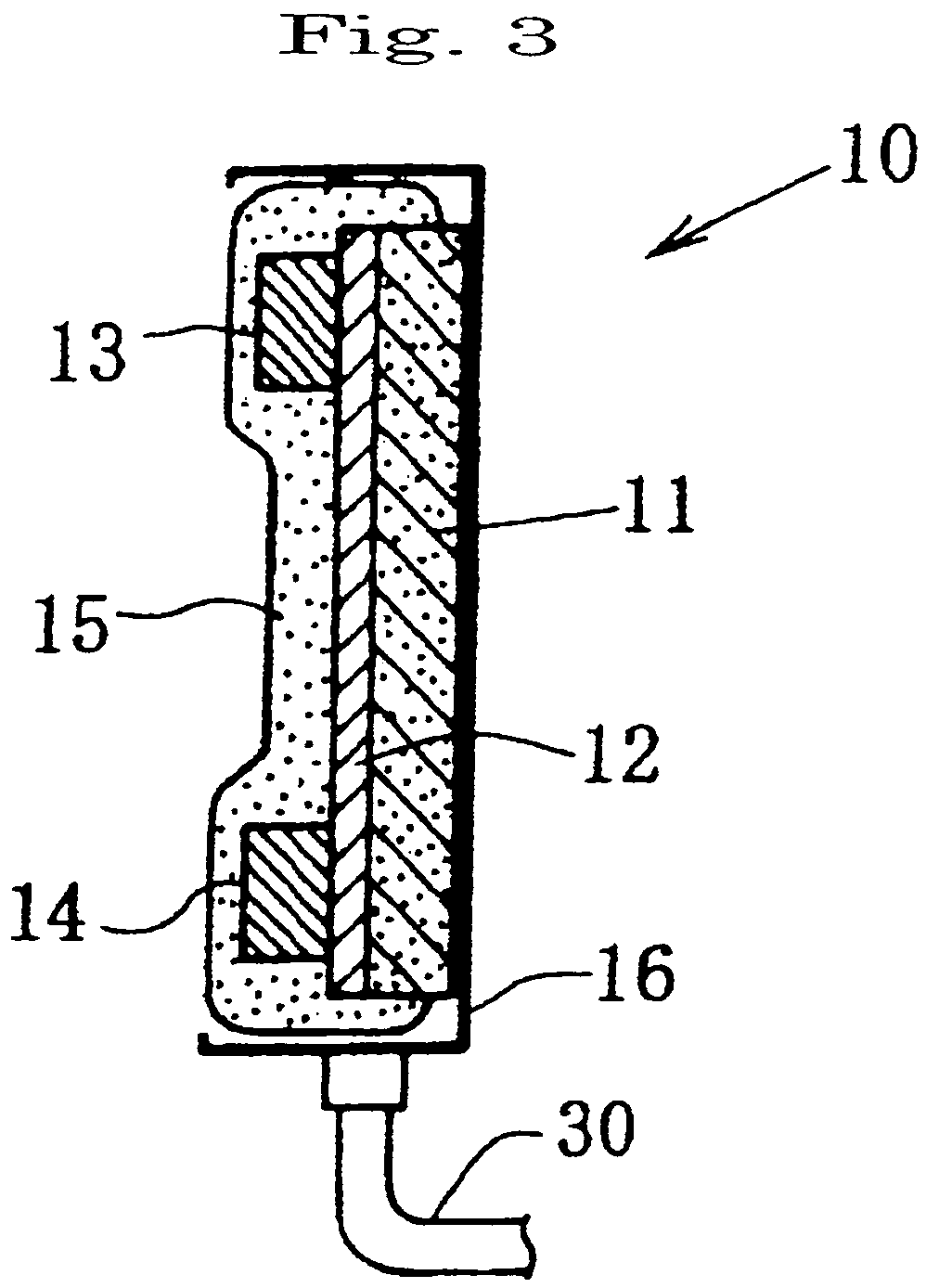
[0028]As shown in FIG. 2 and FIG. 3, the radiation detection element 10 comprises a substrate 11 made of insulating material, a semiconductor layer 12 consisting of a thin film (for example, 250 nm thick) of rutile type titanium oxide formed on the front surface of the substrate 11, a pair of electrodes 13 and 14 connected to the surface of the semiconductor layer 12, an air-tight cover 15, and a metal case 16 covering the back side and the outside of these items.
[0029]The substrate 11 is formed from an insulating material with a superior radiation resistance such as, for example, alumi...
PUM
 Abstract
Description
Claims
Application Information
 - R&D Engineer
- R&D Manager
- IP Professional
- Industry Leading Data Capabilities
- Powerful AI technology
- Patent DNA Extraction
Browse by: Latest US Patents, China's latest patents, Technical Efficacy Thesaurus, Application Domain, Technology Topic, Popular Technical Reports.
© 2024 PatSnap. All rights reserved.Legal|Privacy policy|Modern Slavery Act Transparency Statement|Sitemap|About US| Contact US: help@patsnap.com