Vertical carbon nanotube-field effect transistor and method of manufacturing the same

a field effect transistor and carbon nanotube technology, applied in pulse generators, instruments, pulse techniques, etc., can solve the problems of complex process for forming 3-d gate structures, difficult to modify the structure of gate gates in such a manner, and reach the scaling limits of traditional complementary metal oxide semiconductor (cmos) technology, etc., to achieve better electron mobility

Active Publication Date: 2006-11-07
SAMSUNG ELECTRONICS CO LTD
View PDF4 Cites 19 Cited by
  • Summary
  • Abstract
  • Description
  • Claims
  • Application Information

AI Technical Summary

Benefits of technology

[0009]The present invention provides a vertical carbon nanotube (CNT)-field effect transistor (FET) with a CNT channel completely surrounded by a gate and which is easy to fabricate and provides improved gate controllability and a method of manufacturing the same.
[0014]The CNT used as a channel of the transistor eliminates the need for a doping process and has better electron mobility than silicon.

Problems solved by technology

As the integration density of semiconductor devices increases, traditional complementary metal oxide semiconductor (CMOS) technology reaches limits of scaling.
However, in a Si transistor employing a 3-D gate structure, it is difficult to modify the structure of a gate in such a manner that maximizes the effect of electric field produced by a gate.
In particular, a process for forming a 3-D gate structure becomes complicated since a Si substrate or Si layer with a 3-D structure produced by deposition and patterning is used as a channel.
The primary challenge of this research is to develop a CNT transistor structure that is easy to fabricate and provides good gate controllability and a method for fabricating the same.

Method used


Image

  • Vertical carbon nanotube-field effect transistor and method of manufacturing the same
  • Vertical carbon nanotube-field effect transistor and method of manufacturing the same
  • Vertical carbon nanotube-field effect transistor and method of manufacturing the same

Examples


Embodiment Construction

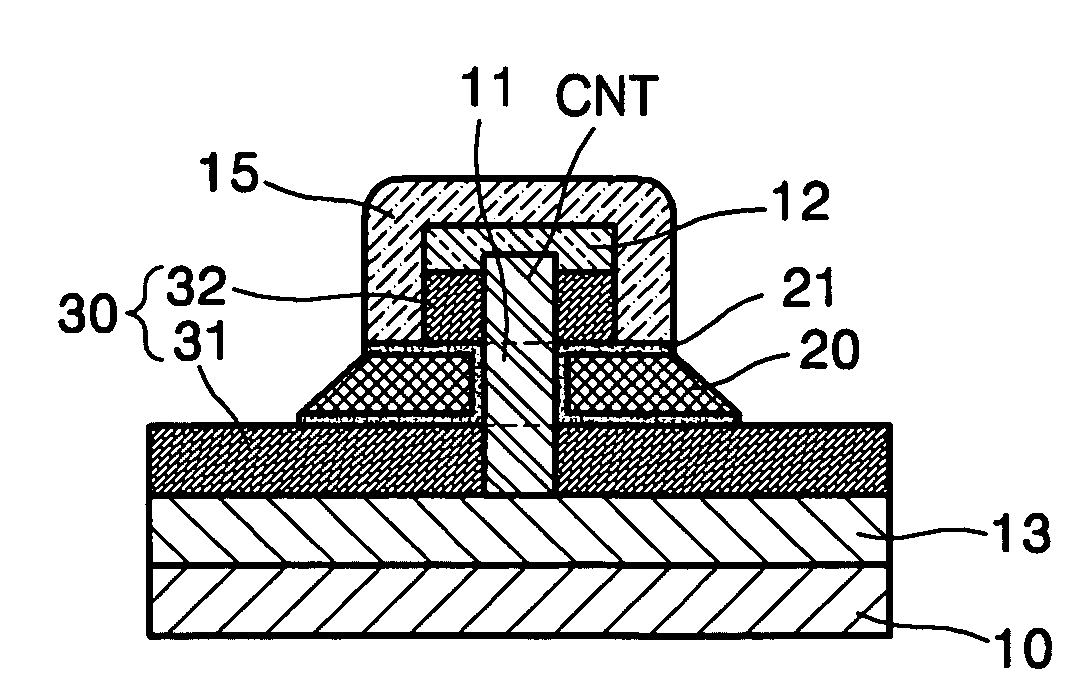
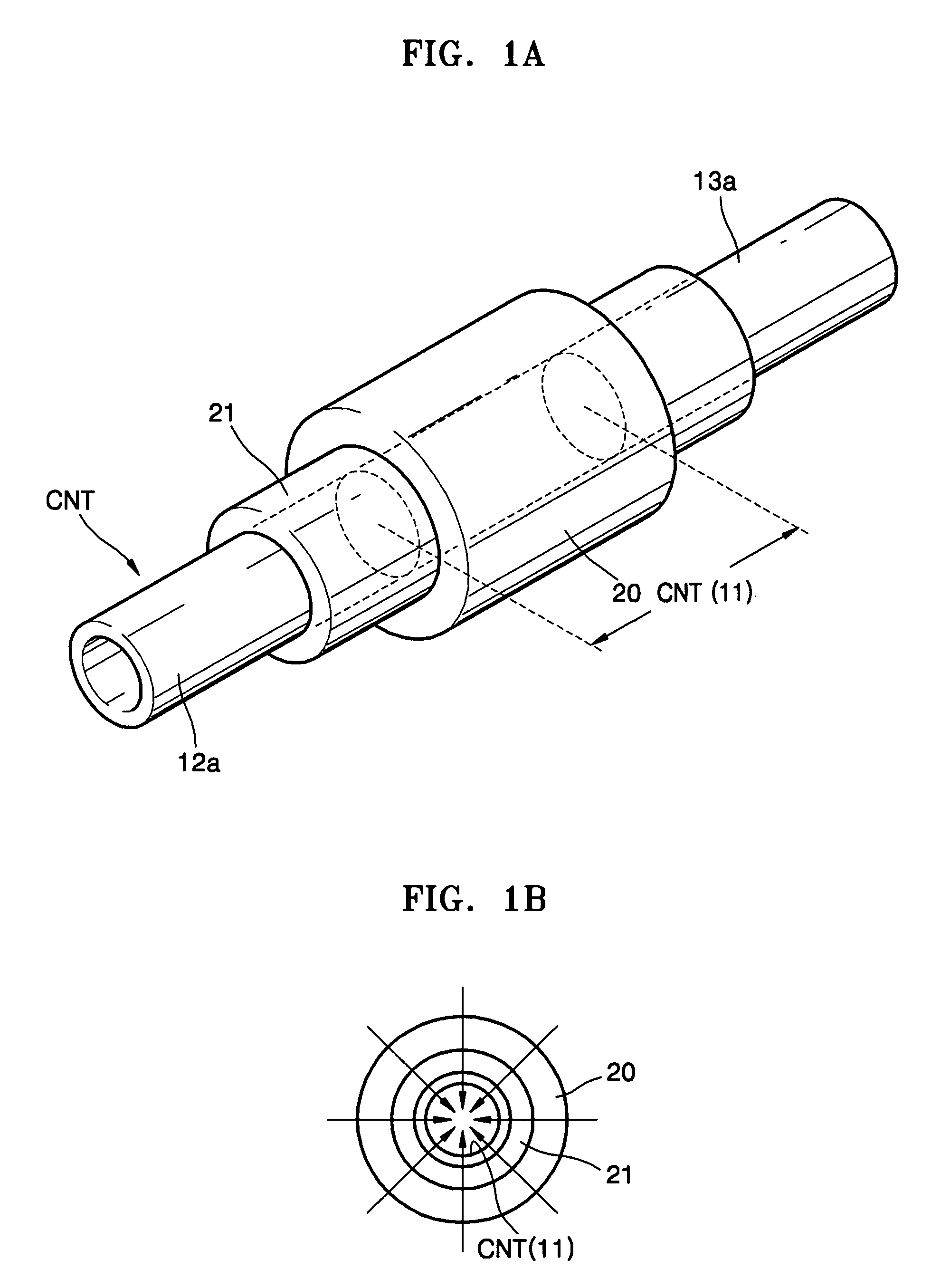
[0025]Referring to FIGS. 1A and 1B, a carbon nanotube (CNT) includes a channel region 11 covered by a gate 20, around which an electric field E is created, and a source 12a and a drain 13a that are placed at either end of the CNT and serve as a simple electrical path. The channel 11, the source 12a, and the drain 13a are defined by the gate 20 enclosing the middle portion of the CNT. A gate insulating layer 21 is interposed between the gate 20 and the channel 11.

[0026]Referring to FIG. 1B, the transistor structure in which the channel 11 is completely enclosed by the gate 20 allows effective creation of an electric field and maximum electric-field effect. Furthermore, the transistor structure maximizes a ratio (Ion / Ioff) of on-current to off-current since a depletion layer formed in the channel 11 by an electric field is isolated from a substrate.

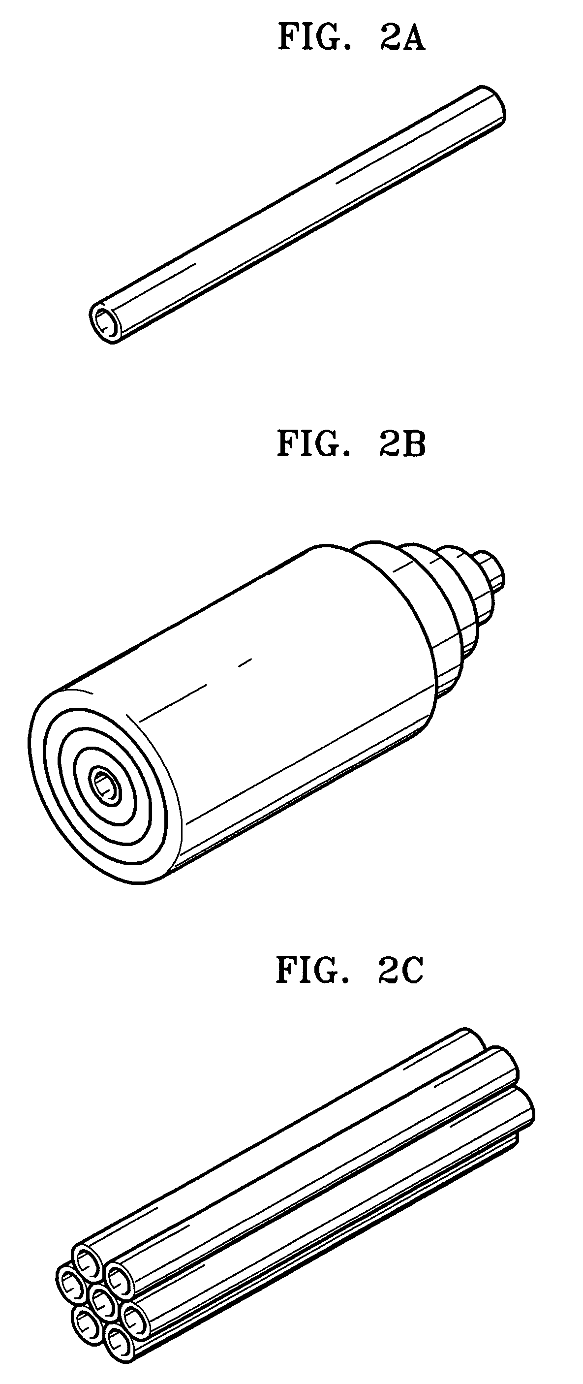
[0027]Depending on a manufacturing process, the CNT comes in common forms as shown in FIGS. 2A–2D. FIGS. 2A–2D respectively show a single-...


PUM


Abstract

Provided are a vertical carbon nanotube field effect transistor (CNTFET) and a method of manufacturing the same. The method includes: forming a first electrode on a substrate; forming a stack of multiple layers (“multi-layer stack”) on the first electrode, the multiple layers including first and second buried layers and a sacrificial layer interposed between the first and second buried layers; forming a vertical well into the multi-layer stack; growing a CNT within the well; forming a second electrode connected to the CNT on the multi-layer stack into which the well has been formed; forming a protective layer on the second electrode; removing the sacrificial layer and exposing the CNT between the first and second buried layers; forming a gate insulating layer on the exposed surface of the CNT; and forming a gate enclosing the CNT on the gate insulating layer. The CNTFET and manufacturing method maximize the effect of electric field produced by the gate due to the channel completely enclosed by the gate while improving a ratio Ion / Ioff of on-current to off-current by fully depleting a depletion layer formed in the channel.

Description

BACKGROUND OF THE INVENTION[0001]Priority is claimed to Korean Patent Application No. 2003-38521, filed on Jun. 14, 2003, in the Korean Intellectual Property Office, the disclosure of which is incorporated herein in its entirety by reference.[0002]1. Field of the Invention[0003]The present invention relates to a vertical carbon nanotube (CNT)-field effect transistor (FET) and a method of manufacturing the same, and more particularly, to a vertical CNT-FET employing a CNT channel surrounded by a gate and a gate insulating layer and a method of manufacturing the same.[0004]2. Description of the Related Art[0005]As the integration density of semiconductor devices increases, traditional complementary metal oxide semiconductor (CMOS) technology reaches limits of scaling. High integration, high performance, and low power dissipation are achieved by reducing the dimensions of CMOS devices. This trend comes with decreases in the width and length of a gate electrode, an isolation area betwee...

Claims


Application Information

Patent Timeline
Patent Type & Authority Patents(United States)
IPC IPC(8): H01L29/76H01L29/772H01L51/30H03K3/037H03K3/12H03K3/286
CPCB82Y10/00H01L51/0048H01L51/057G11C2213/18H10K85/221H10K10/491H01L29/772
Inventor BAE, EUN-JUMIN, YO-SEPPARK, WAN-JUN
Owner SAMSUNG ELECTRONICS CO LTD
Why Eureka
Try Eureka