Semiconductor device manufacture method capable of supressing gate impurity penetration into channel

a technology of impurity penetration and manufacture method, which is applied in the direction of semiconductor devices, electrical devices, transistors, etc., can solve the problems of increasing leak current, reducing the operation speed of capacitance, and limited active region area, so as to increase the capacitance of source/drain region, increase the leak current, and increase the effect of leak curren

Inactive Publication Date: 2006-11-14
FUJITSU SEMICON LTD
View PDF13 Cites 9 Cited by
  • Summary
  • Abstract
  • Description
  • Claims
  • Application Information

AI Technical Summary

Benefits of technology

[0023]It is an object of the present invention to provide a semiconductor device manufacture method capable of suppressing impurity ions implanted into a gate electrode from penetration through a gate insulating film and suppressing an increase in capacitance of source / drain regions and an increase in leak current.
[0024]It is another object of the present invention to provide a semiconductor device manufacture method capable of suppressing impurity ions implanted into a gate electrode having a limited height from penetration through a gate insulating film and forming source drain region junctions deeper.
[0025]It is still another object of the present invention to provide a semiconductor device manufacture method capable of suppressing a threshold voltage variation, and reducing parasitic capacitance of source / drain regions and leak current.

Problems solved by technology

If element isolation is formed by local oxidation of silicon (LOCOS), bird's beaks are formed gradually thickening the oxide film so that an area of an active region and hence an integration degree are limited.
An increase in capacitance lowers the operation speed.
Further, a shallow junction increases leak current.
If the effective thickness of the source / drain regions becomes thin, leak current is likely to flow through the source / drain junctions.
As described above, the shallow source / drain regions result in an increase in capacitance and leak current and a serious obstacle against a circuit operation.
This is the main cause of leak current, among others.

Method used


Image

  • Semiconductor device manufacture method capable of supressing gate impurity penetration into channel
  • Semiconductor device manufacture method capable of supressing gate impurity penetration into channel
  • Semiconductor device manufacture method capable of supressing gate impurity penetration into channel

Examples


Embodiment Construction

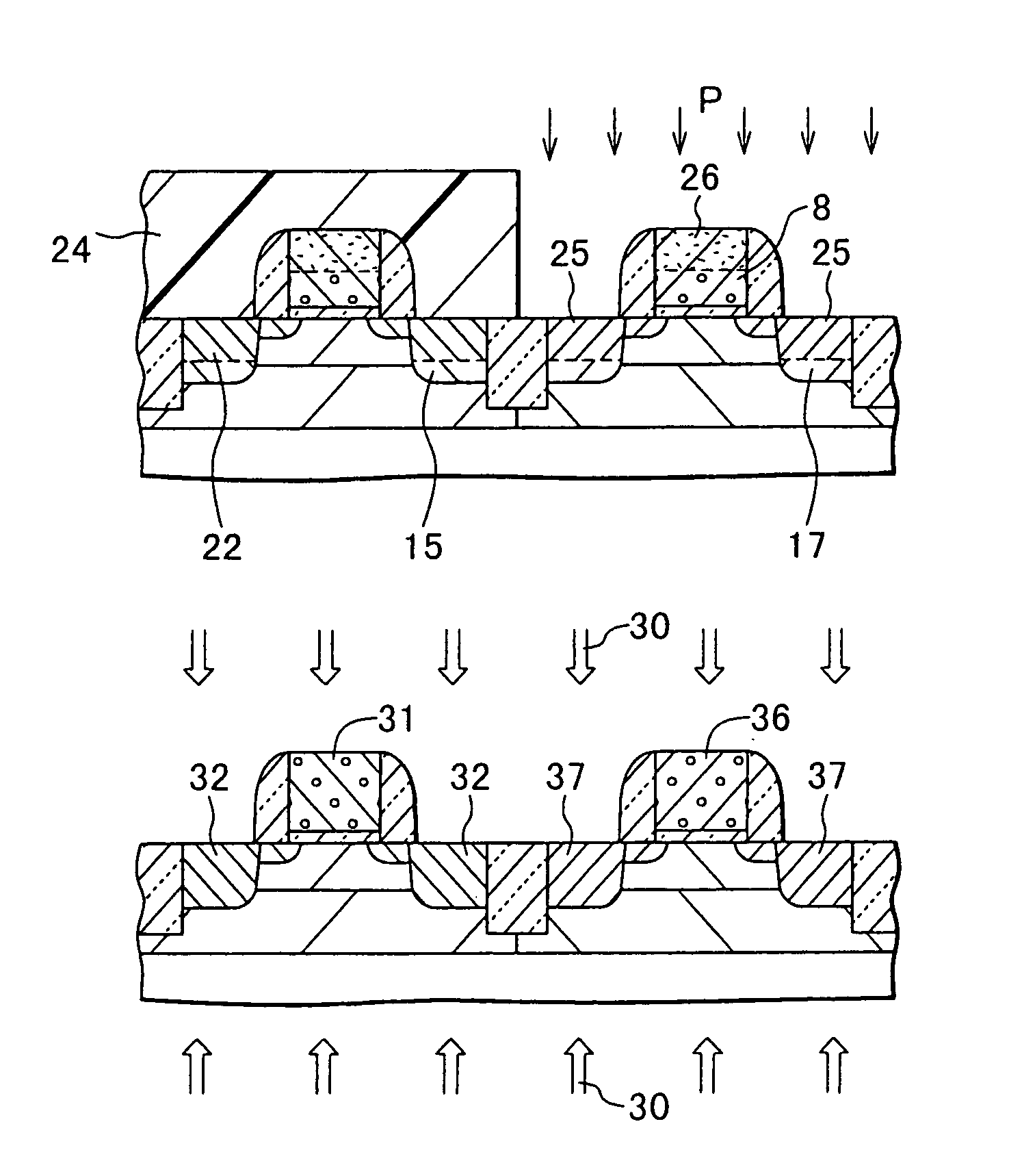
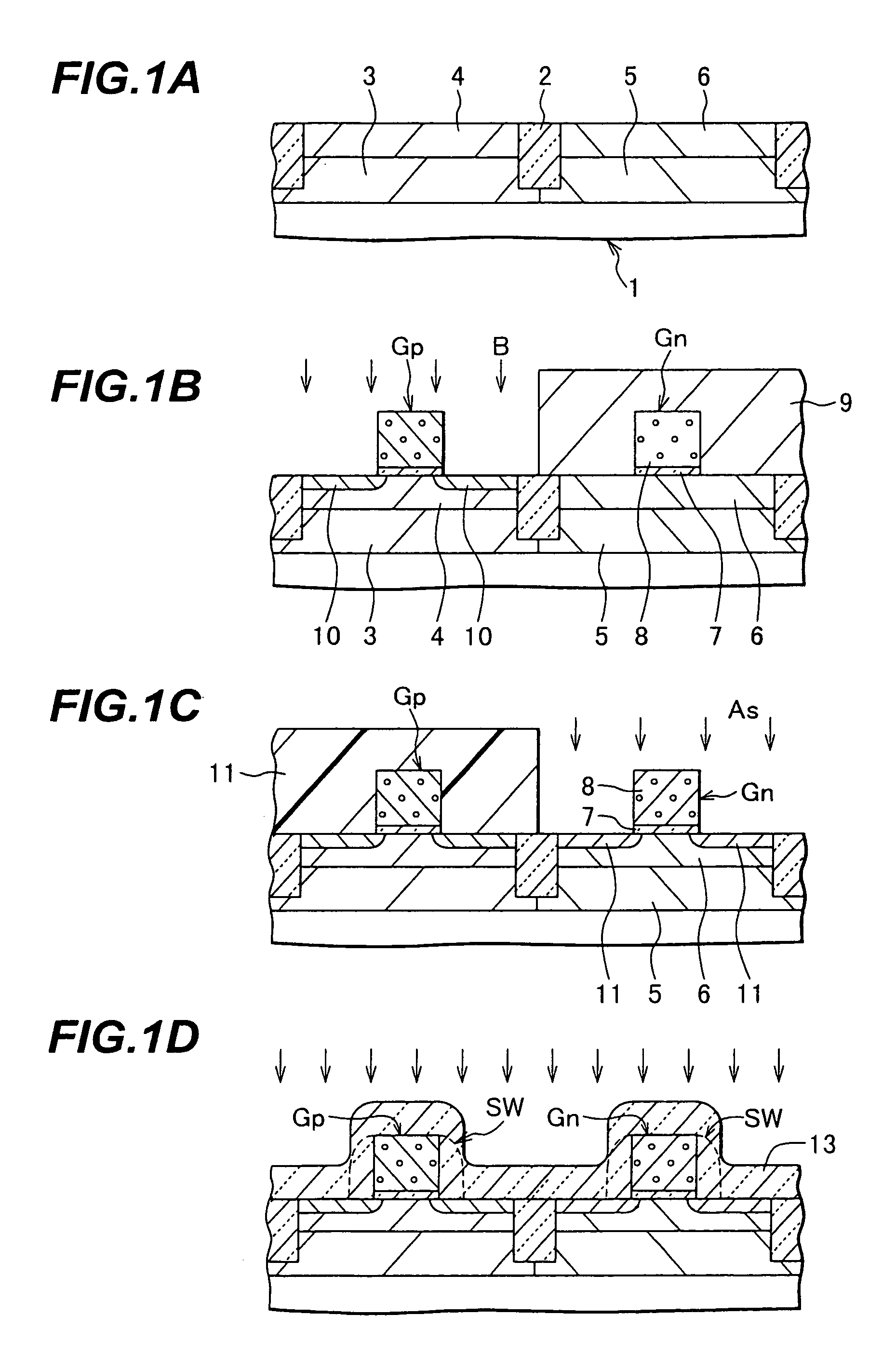
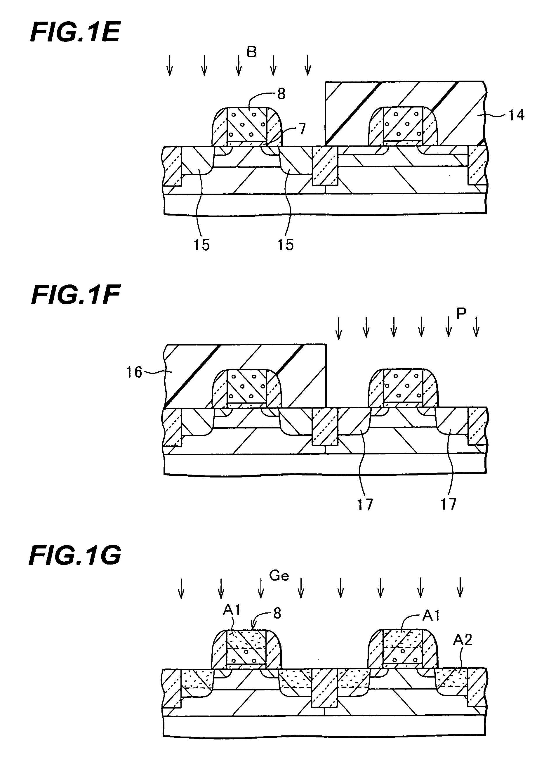
[0033]Prior to the description of embodiments of the present invention, the characteristics of ion implantation will be described as background art.

[0034]FIG. 5A is a graph showing the characteristics of ion implantation into single crystal silicon and poly-silicon. Different behaviors can be seen if ions are implanted into single crystal silicon and poly-silicon at a high impurity concentration and a relatively low acceleration energy of, for example, 3 to 5 keV.

[0035]FIG. 5A is a graph showing an impurity concentration distribution when B ions are implanted into single crystal and poly-silicon at an acceleration energy of 5 keV and a dose of 1×1015 cm−2. In FIG. 5A, the abscissa represents a depth from a surface in the unit of nm, and the ordinate represents a concentration of implanted B ions in the unit of cm−3 in a logarithmic scale.

[0036]A curve s1 indicates an impurity concentration distribution when B ions are implanted into single crystal silicon along a substrate plane nor...


PUM


Abstract

A gate electrode is formed above an n-type well including an n-type threshold voltage adjustment region, ions of p-type impurity are implanted with a low acceleration energy to form extension regions in the n-type well on both sides of the gate electrode, side wall spacers are formed on the side walls of the gate electrode, ions of p-type impurity are implanted with a small dose causing substantially no abnormal tailing in the gate electrode and with a relatively high acceleration energy to form p-type source / drain regions deeper than the threshold adjustment region, ions of atoms are implanted into the semiconductor substrate to change the upper parts of the gate electrode and the source / drain regions to amorphous state, ions of p-type impurity are implanted with a large dose to form high-concentration parts in the source / drain regions, and the impurities introduced by the ion implantation are activated.

Description

CROSS REFERENCE TO RELATED APPLICATION[0001]This application is a continuation application of an International Patent Application PCT / JP2003 / 005560 filed on Apr. 30, 2003, the entire contents of which are incorporated herein by reference.BACKGROUND OF THE INVENTION[0002](A) Field of the Invention[0003]The present invention relates to a semiconductor device manufacture method, and more particularly to a method of manufacturing a semiconductor device having very fine transistors.[0004](B) Related Art[0005]Semiconductor integrated circuit devices are at the stage of higher integration degree and operation speed. Constituent elements of a semiconductor integrated circuit device, MOS transistors, are becoming very fine in accordance with the scaling rules. The gate insulating film becomes thin and the gate length becomes short. The height of the gate electrode is limited.[0006]As the gate length becomes short, carriers can punch through from the source to drain and the short channel effe...

Claims


Application Information

Patent Timeline
Patent Type & Authority Patents(United States)
IPC IPC(8): H01L21/265H01L21/3205H01L21/336H01L21/425H01L21/28H01L21/8238H01L29/08H01L29/78H01L31/109
CPCH01L21/26506H01L21/28035H01L21/823807H01L21/823835H01L21/823842H01L21/823864H01L29/0847H01L29/665H01L29/6659H01L29/7833H01L21/26513
Inventor TAGAWA, YUKIO
Owner FUJITSU SEMICON LTD
Why Eureka
Try Eureka