Boron-doped nanocrystalline diamond
a nanocrystalline diamond and boron-doped technology, applied in the field of boron-doped nanocrystalline diamonds, can solve the problems of low quality and achieve the effect of improving conductivity
- Summary
- Abstract
- Description
- Claims
- Application Information
AI Technical Summary
Benefits of technology
Problems solved by technology
Method used
Image
Examples
Embodiment Construction
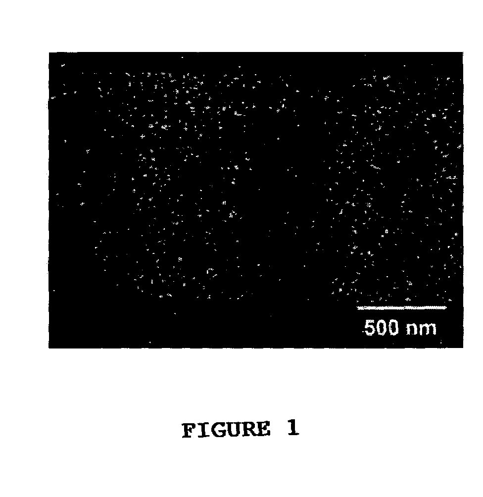
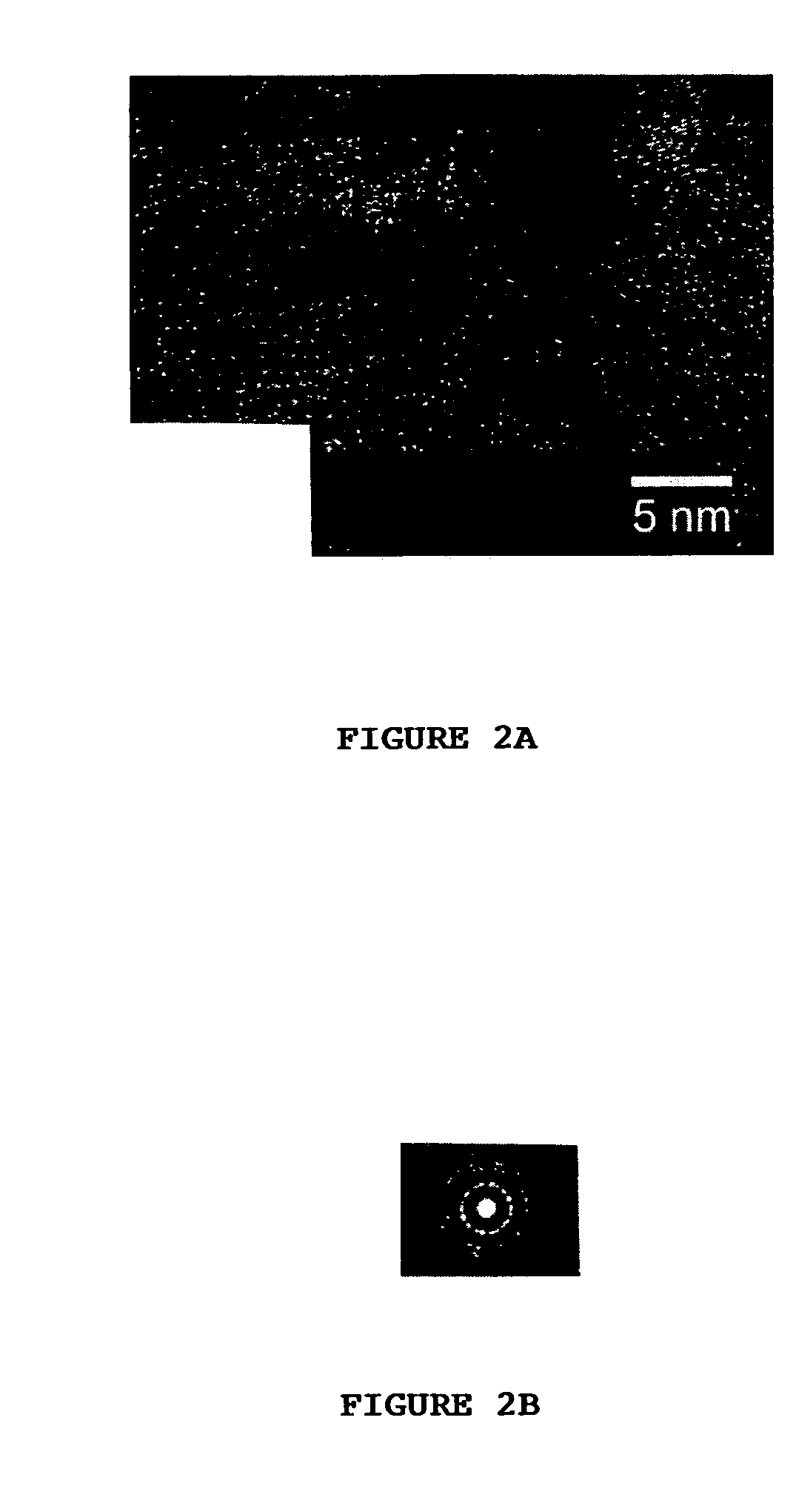
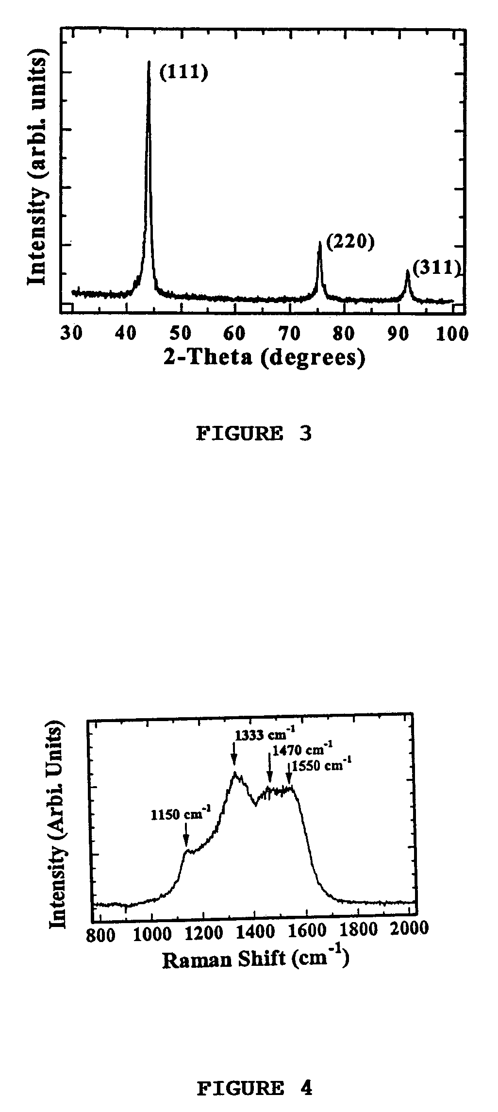
[0028]The present invention involves boron-doped, phase pure nanocrystalline diamond thin films. The most remarkable difference in films grown using hydrogen-poor Ar gas mixtures, compared with conventional hydrogen-rich mixtures, is the nanocrystallinity of the former compared with the microcrystallinity of the latter. The nanocrystallinity is a result of a growth and nucleation mechanism involving the insertion of carbon dimer, C2, into surface C—H bonds. The C2 addition is believed to occur by a two-step growth mechanism (McCauley, T. G., et al., Appl. Phys. Lett. 73 1646 (1998)). A C2 molecule approaches the unreconstructed monohydride surface and inserts into a C—H bond. The C2 molecule then rotates to insert its other carbon into a neighboring C—H bond on the surface. A C2 molecule then inserts into an adjacent C—H bond, parallel to the newly inserted C2 dimer. The original state of the surface is recovered by the formation of a bond between carbon atoms in the adjacent surfac...
PUM
| Property | Measurement | Unit |
|---|---|---|
| temperature | aaaaa | aaaaa |
| pressure | aaaaa | aaaaa |
| grain size | aaaaa | aaaaa |
Abstract
Description
Claims
Application Information


