
Switching power supply circuit

a power supply circuit and switching technology, applied in the direction of electric variable regulation, process and machine control, instruments, etc., can solve the problems of increasing the number of components, the upper limit of the driving frequency for which the switching driving circuit is ready is approximately 200 khz, and the inability to use the switching driving circuit practically as an actual power supply circuit, etc., to achieve the effect of reducing the control range of the switching frequency, enhancing the responsibility for constant voltage control, and high degree of reliability

Inactive Publication Date: 2006-12-05
SONY CORP
View PDF8 Cites 7 Cited by
  • Summary
  • Abstract
  • Description
  • Claims
  • Application Information

AI Technical Summary

Benefits of technology

[0075]The switching power supply circuits each adopts a configuration of a switching converter in which a primary side series resonance circuit which makes a switching operation of the primary side that of the current resonance type is formed, and includes a series resonance circuit formed also on the secondary side. Where the switching power supply circuit has the configuration just described, if the gap length of the gap formed in the core of the insulating converter transformer whose electromagnetic coupling is utilized to form a coupling type resonance circuit is set to a predetermined length to obtain a predetermined coupling coefficient, then a steep single-humped characteristic can be obtained as an output characteristic for an alternating voltage of a switching frequency which is an input to the coupling type resonance circuit. As a result, when compared with an alternative configuration wherein a series resonance circuit is formed only on the primary side, the variable range (necessary control range) of the switching frequency necessary for stabilization can be reduced.
[0084]Further, if the current level to flow in the secondary windings can be reduced, then also the current withstanding property of the rectification elements on the secondary side can be reduced, and consequently, reduction of the circuit board area can be achieved using a rectification element of a reduced size.

Problems solved by technology

However, in an existing IC (oscillation and driving circuit 2) for driving a switching device, the upper limit to the driving frequency for which it is ready is approximately 200 kHz.
Therefore, the switching driving IC cannot be practically used as an actual power supply circuit.
Therefore, the cost is increased by increase of the number of components and also the mounting area of a circuit board of the power supply circuit is increased, which increases the scale of the power supply circuit.
Particularly, since the smoothing capacitors and the electromagnetic relays are large among various components for forming the power supply circuit, the size of the circuit board becomes considerably great.
Therefore, the resulting voltage exceeds the withstanding voltage, for example, of the switching devices Q1 and Q2, and as a result, there is the possibility that the switching devices Q1 and Q2 may be broken.
Consequently, components for detecting the converter circuit on the standby power supply circuit side are additionally provided, and as a result, increase of the cost and increase of the size of the circuit board described above are further promoted.
In particular, the type of an electronic apparatus capable of incorporating the power supply is limited to that of an electronic apparatus which includes a standby power supply, and as a result, the utilization range decreases as much.
Further, since the changeover in the configuration is not that on the commercial power supply line and the circuit form can be changed over by a semiconductor switch, a large-size switching member such as an electromagnetic relay need not be provided.
While the resonance converter can be operated with low switching noise, as the number of switching devices which perform switching in this manner increases, the disadvantage increases as regards switching noise.
Also where any one of the configurations described above is adopted as a configuration ready for the wide range, when compared with a configuration ready for a single range, increase of the cost and increase of the circuit size arising from increase of the number of parts or the like cannot be avoided.
Further, new problems which do not appear with the configuration ready for a single range such as a limit to the utilization range to equipment in the case of the former configuration and increase of switching noise in the case of the latter configuration and so forth appear.
Further, where the control range of the switching frequency is suitably wide as in the power supply circuit shown in FIG. 14, also a problem appears that the high speed response characteristic of stabilization of the secondary side DC output voltage Eo degrades.
However, where the control range of the switching frequency is wide as described with reference to FIG. 17, in order to adjust the switching frequency to a switching frequency with which the secondary side DC output voltage is adjusted to a required level in response to the load variation of a load like such a switching load as described above, a comparatively long period of time is required.
In short, an unfavorable result is obtained as the response characteristic of the constant voltage control.
Particularly, as shown in FIG. 16, as the switching frequency characteristic by constant voltage control by the power supply circuit shown in FIG. 14, the switching frequency varies by a great amount within the load range of the load power Po from Po=approximately 25 W to Po=0 W. Therefore, it is recognized that the power supply circuit is disadvantageous in the responsibility in constant voltage control for such a switching load as described above.

Method used


Image

  • Switching power supply circuit
  • Switching power supply circuit
  • Switching power supply circuit

Examples


first embodiment

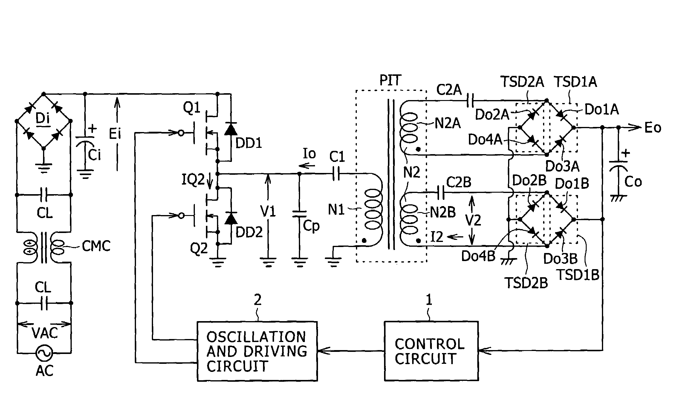
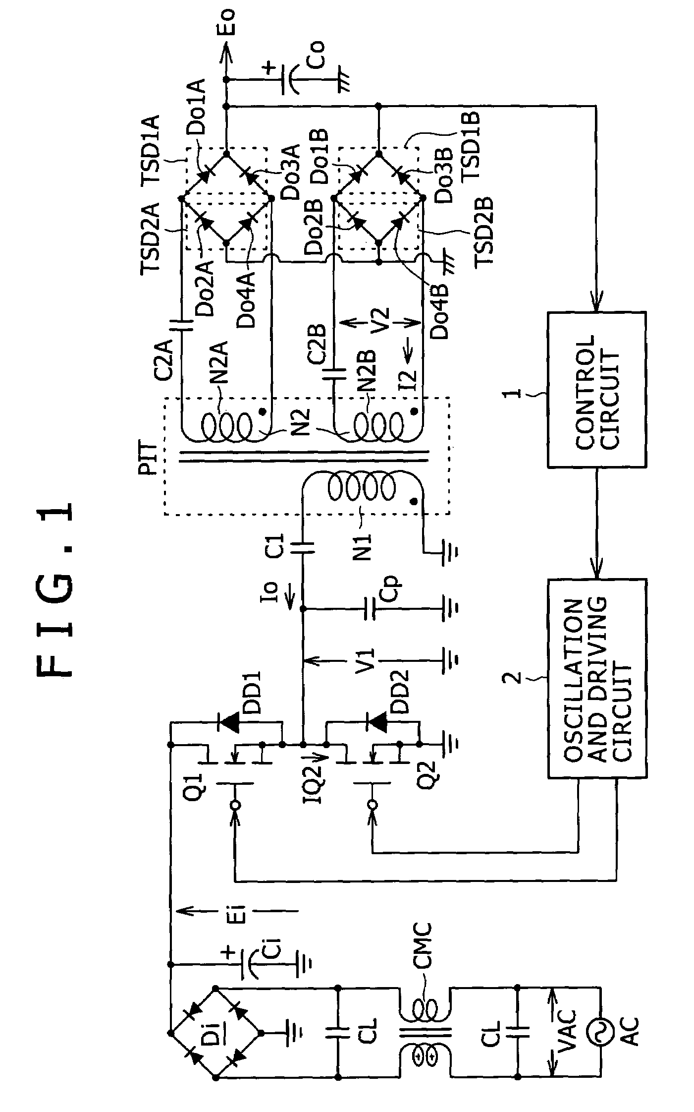
[0104]The power supply circuit of the present first embodiment has a configuration ready for the wide range by which it operates with both of commercial AC power supply inputs of the AC 100 V type and the AC 200 V type. Further, as regards the applicable load power, the power supply circuit is ready for a variation range of the load power Po, for example, from Po=approximately 150 W to 0 W (no load). Also in this instance, an secondary side DC output voltage Eo of, for example, approximately 25 V is obtained similarly as in the case of the circuit described hereinabove with reference to FIG. 14.

[0105]In particular, in the power supply circuit shown in FIG. 1, a common mode noise filter is formed from a pair of filter capacitors CL and a common mode choke coil CMC for a commercial AC power supply AC.

[0106]A full-wave rectification smoothing circuit is connected to the commercial AC power supply AC at the next stage to the noise filter. The full wave rectification smoothing circuit is...

second embodiment

[0285]It is to be noted that the pertaining elements of the power supply circuit of the second embodiment shown in FIG. 11 were selectively set in the following manner:[0286]insulating converter transformer PIT: gap G=1.6 mm, coupling coefficient k=0.65[0287]primary winding N1=42 T[0288]secondary winding N2A=N2A1+N2A2=2 T+2 T=4 T[0289]secondary winding N2B=N2B1+N2B2=2 T+2 T=4 T[0290]primary side series resonance capacitor C1=0.033 μF[0291]secondary side series resonance capacitor C2A1=C2A2=C2B1=C2B2=1.0 μF

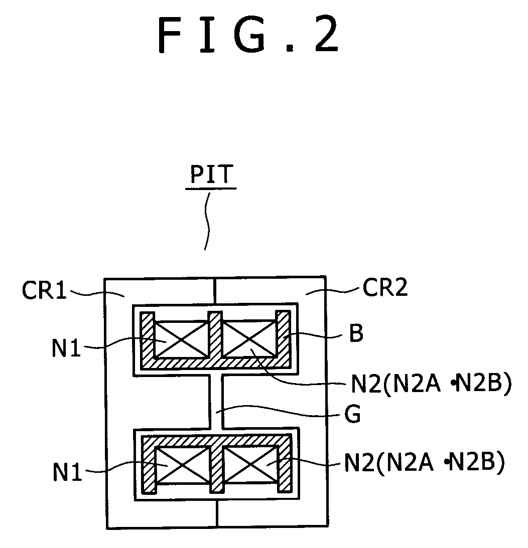
[0292]In short, also in the second embodiment, in order to set the coupling coefficient k to k=approximately 0.65, for example, a gap length of approximately 1.6 mm is set for the gap G formed in the inner magnetic leg of the core of the insulating converter transformer PIT of the structure shown in FIG. 2 similarly as in the power supply circuit of the first embodiment shown in FIG. 1.

[0293]This achieves a configuration ready for the wide range.

[0294]Further, by such setting of th...


PUM


Abstract

A power supply circuit is disclosed which performs constant voltage control by switching frequency control and is ready for a wide range while the necessary control range of the switching frequency control is reduced. The circuit includes a primary side series resonance circuit forming a current resonance type converter, and a secondary side series resonance circuit formed from secondary windings and secondary side series resonance capacitors while a coupling type resonance circuit by electromagnetic coupling of an insulating converter transformer is formed. To obtain a single-humped characteristic from the coupling type resonance circuit, a gap of approximately 1.6 mm is formed in the core of the insulating converter transformer so as to achieve a coupling coefficient of 0.65 or less. A secondary side DC output voltage is produced from outputs of the secondary windings so as to cope with a heavy load condition.

Description

CROSS REFERENCES TO RELATED APPLICATIONS[0001]The present invention contains subject matter related to Japanese Patent Application JP 2004-271920 filed in the Japanese Patent Office on September, 2004, the entire contents of which being incorporated herein by reference.BACKGROUND OF THE INVENTION[0002]This invention relates to a switching power supply circuit which is provided as a power supply in various pieces of electronic equipment.[0003]Meanwhile, the assignee of the present patent application has proposed various power supply circuits wherein a resonance type converter is provided on the primary side.[0004]FIG. 14 is a circuit diagram showing an example of a switching power supply circuit which includes a resonance type converter and is formed based on the invention applied for patent in advance by the assignee of the present application.[0005]Referring to FIG. 14, the power supply circuit shown includes a switching converter configured such that a partial voltage resonance ci...

Claims


Application Information

Patent Timeline
Patent Type & Authority Patents(United States)
IPC IPC(8): H02M3/335H02M3/28H02M7/5383
CPCH02M3/3376H02M2001/0058Y02B70/1491H02M1/0058Y02B70/10H02M3/28
Inventor YASUMURA, MASAYUKI
Owner SONY CORP
Learn More