Apparatus for optical measurements on low-index non-solid materials based on arrow waveguides

a technology of arrow waveguides and optical measurements, applied in the field of integrated optics, can solve the problems of large parallelism, inability to easily scale up to multiple sample volumes, and bulky setups in natur

Active Publication Date: 2006-12-12
BRIGHAM YOUNG UNIV +1
View PDF13 Cites 60 Cited by
  • Summary
  • Abstract
  • Description
  • Claims
  • Application Information

AI Technical Summary

Benefits of technology

[0016]In a presently preferred embodiment of the invention, an optical waveguide is constructed so as to comprise a non-solid core layer surrounded by a solid-state material. In particular, unlike the micromachined structure disclosed by Bernini, et al., in “Silicon Micromachined Hollow Optical Waveguides for Sensing Applications”, supra, the optical waveguide includes a substrate and multiple layers of solid state material disposed on the substrate, and a non-solid core extending through at least one of the multiple layers. The substrate can be made of Silicon (Si) or other solid material. The waveguides in question could be made on different semiconductor substrates but also on a smooth metal, ceramic, or plastic surface. The non-solid core may be used to contain a sample material whose light transmission, absorption, and / or interference characteristics are to be measured. The sample may have an index of refraction which is lower than the index of refraction of the surrounding solid-state material, and light can be transmitted with low loss through the non-solid core layer and sample material.

Problems solved by technology

Problems associated with this method include the fact that only extremely small volumes on the order of fl are tolerable, and more importantly, that such setups are bulky in nature and cannot be scaled readily to multiple sample volumes.
However, while this method is clearly ingenious, it can be seen from FIG.
1(b) that the setup is still rather cumbersome and involves optical paths for excitation and detection that are perpendicular to the sample plane.
The metal film contains a large number of these zero-mode waveguides, which results in large parallelism.
However, since the fluorescence is collected through a microscope objective, a large number of these holes are interrogated simultaneously and deliberate readout from a single hole is impossible.
However, it is highly inefficient as it relies on detection of exponentially decaying electric field values of the fluorescence signal.
As a result, no transport of the optical signal through a waveguide or all-optical post-processing is possible.
This arrangement brings with it significant loss of the optical signal due to multiple interfaces between the sample space and the end of the microscope objective.
However, they intersect an ordinary microcapillary which again leads to significant coupling losses into and out of the capillary leading to a coupling efficiency of only a few percent.
However, such structures are extremely complicated to fabricate and cannot be used for some of the applications of interest here.
Single-mode propagation and light confinement in gases is not possible with this approach.

Method used


Image

  • Apparatus for optical measurements on low-index non-solid materials based on arrow waveguides
  • Apparatus for optical measurements on low-index non-solid materials based on arrow waveguides
  • Apparatus for optical measurements on low-index non-solid materials based on arrow waveguides

Examples


Embodiment Construction
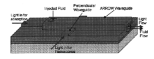
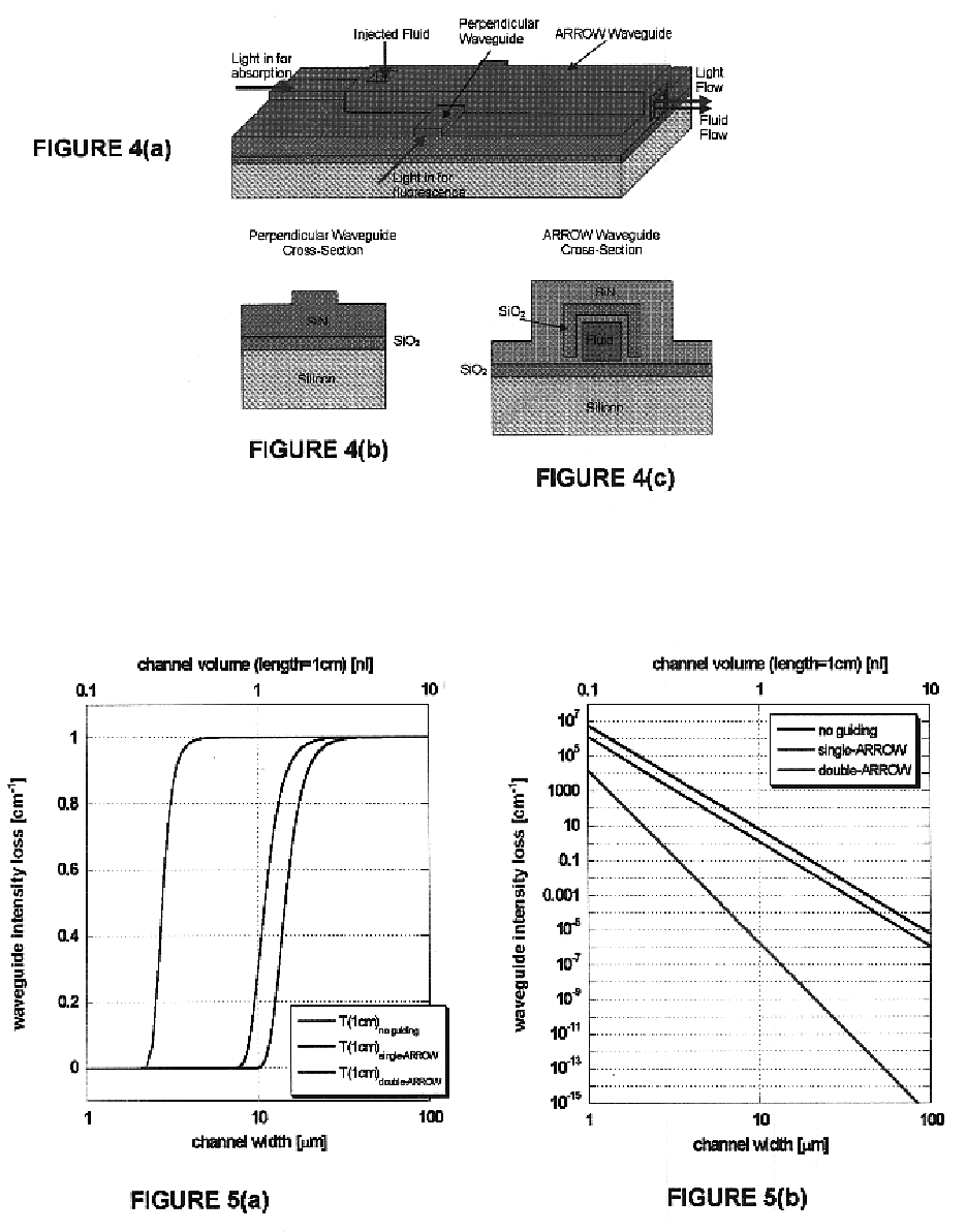
[0046]Overview

[0047]Currently, cutting edge optical studies of biological agents such as DNA molecules or cells do not take advantage of the established technologies that have made optoelectronic and photonic integrated circuits so successful. Optical setups for biomedical applications typically involve bulky three-dimensional setups and often times the use of microscope objectives for excitation and / or collection. The main reason behind this fact is the inability to guide light through the media in which the cells and molecules are hosted (typically aqueous solutions or gas phase), as these media have lower refractive indices than the surrounding solid-state material.

[0048]Here, we present the invention of a radically different approach to creating an experimental platform for optical studies on non-solid-state materials. By using specially designed multi-layer optical waveguides, it is possible to guide light through low-index media over macroscopic distances which will enable opt...


PUM

PropertyMeasurementUnit
widthaaaaaaaaaa
diameteraaaaaaaaaa
lengthaaaaaaaaaa

Abstract

An optical waveguide is constructed so as to comprise a non-solid core layer surrounded by a solid-state material. The non-solid core layer has an index of refraction which is lower than the index of refraction of the surrounding solid-state material, and light can be transmitted with low loss through the non-solid core layer. In an exemplary application, the non-solid core layer comprises a sample material whose light transmission, absorption, and/or interference characteristics are to be measured. In addition, a perpendicular waveguide portion may be included for use in injecting light into the core for measuring fluorescence characteristics associated with the sample material. Most preferably, the optical waveguide is generally structured as an anti-resonant reflecting optical waveguide (ARROW), which comprises a Fabry-Perot reflector adjacent to the core layer, whereby light is substantially prevented from leaking out of said core in a transverse direction.

Description

CROSS REFERENCE[0001]This application claims the benefit of the filing date of U.S. Provisional Application No. 60 / 479,376, filed Jun. 16, 2003, “Apparatus For Optical Measurements On Low-Index Non-Solid Materials Based On Arrow Waveguides,” which is hereby incorporated by reference in its entirety.FIELD OF THE INVENTION[0002]The present invention relates generally to the field of integrated optics, and more particularly to an optical waveguide comprising a non-solid core layer surrounded by a solid-state material, wherein light can be transmitted with low loss through the non-solid core layer. A presently preferred implementation of the invention employs anti-resonant reflecting optical waveguides, known as ARROWs or ARROW waveguides.BACKGROUND OF THE INVENTION[0003]Our invention provides a practical way to extend the field of integrated optics to non-solid waveguide core materials. That is, we describe a way for guiding light on a chip through non-solid materials such as gases and...

Claims


Application Information

Patent Timeline
Patent Type & Authority Patents(United States)
IPC IPC(8): G01N21/00G02B6/10G01N21/03G01N21/05G01N21/59G01N21/64G02B6/122
CPCG01N21/0303G01N21/05G01N21/59G01N21/645G01N21/6486G02B6/122G02B2006/0325G01N2021/0346
Inventor SCHMIDT, HOLGERHAWKINS, AARON ROE
Owner BRIGHAM YOUNG UNIV
Why Eureka
Try Eureka