Giant remnant polarization in laser ablated SrBi2Nb2O9 thin films on Pt/TiO2/SiO2/Si substrates

Active Publication Date: 2007-01-02
PUERTO RICO UNIV OF
View PDF0 Cites 2 Cited by
  • Summary
  • Abstract
  • Description
  • Claims
  • Application Information

AI Technical Summary

Benefits of technology

[0012]According to a more preferred aspect of the invention, the compound has a maximum remnant polarization of at least 40 μC/cm2.
[0013]According to a still more preferred aspect of the invention, the compound has a maximum remnant polarization of at least approximately 50 μC/cm2.
[0014]According to another aspect of the invention, a thin film having a high remnant polarization is fabricated. A platinum-coated silicon substrate is provided. The platinum-coated silicon substrate is composed of layers of Pt/TiO2/SiO2/Si. A layer of SrBi2Nb2O9 is deposited on the platinum-coated silicon substrate by pulsed laser deposition to

Problems solved by technology

Fatigue (defined as loss of polarization with repeated switching of the field) and imprint are the principle factors limiting commercialization of PZT based NVRAMs.
This fabrication, however, presents another problem.
The integration of oxide electrodes in Si technology complicates the design rules for various commonly-used interconnections.
Unfortunately, however, some of the intrinsic fundamental material problems associated with SBT include: (1) a low remnant polarization (Pr=10 μC / cm2); (2) a relatively high crystallization temperature (˜750° C.

Method used


Image

  • Giant remnant polarization in laser ablated SrBi2Nb2O9 thin films on Pt/TiO2/SiO2/Si substrates
  • Giant remnant polarization in laser ablated SrBi2Nb2O9 thin films on Pt/TiO2/SiO2/Si substrates
  • Giant remnant polarization in laser ablated SrBi2Nb2O9 thin films on Pt/TiO2/SiO2/Si substrates

Examples


Embodiment Construction

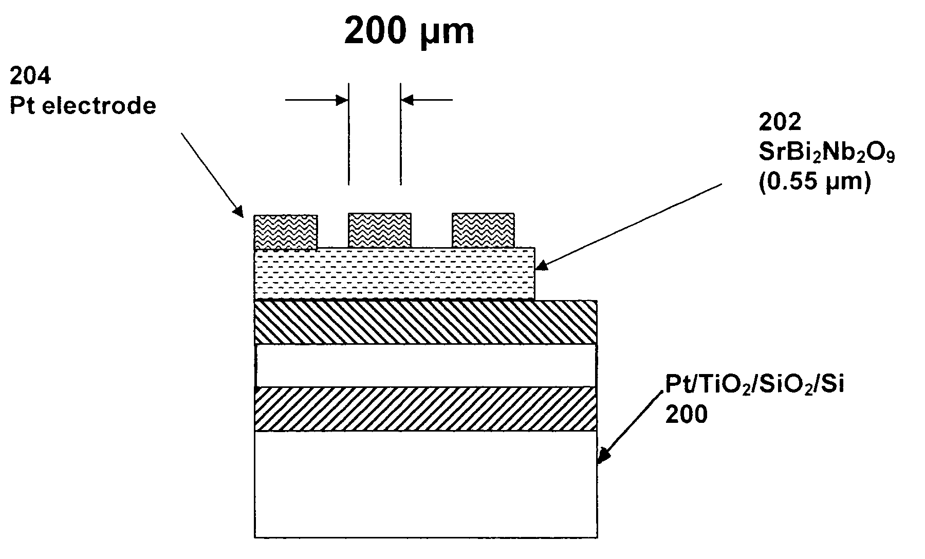
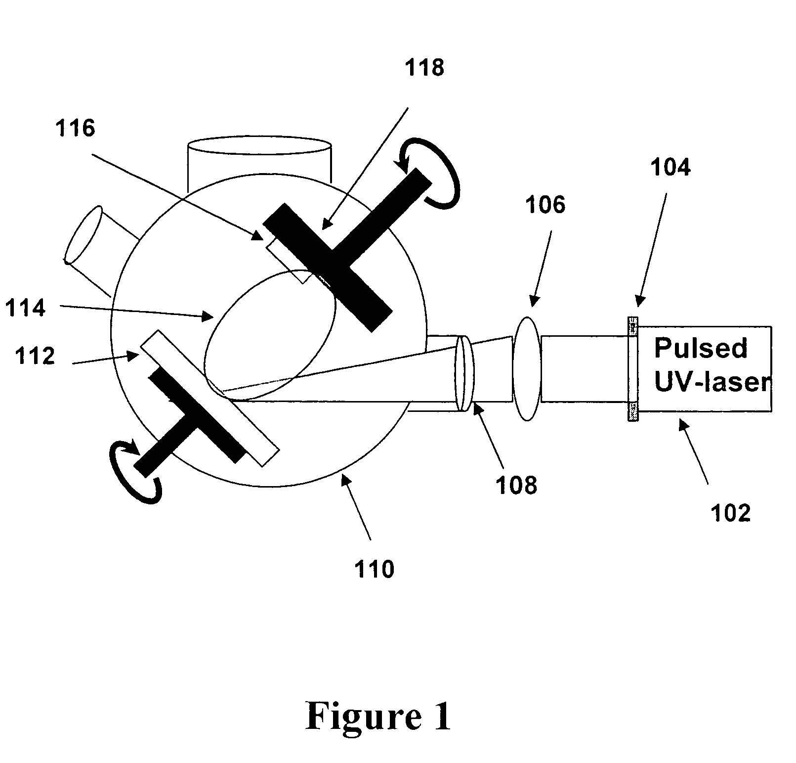
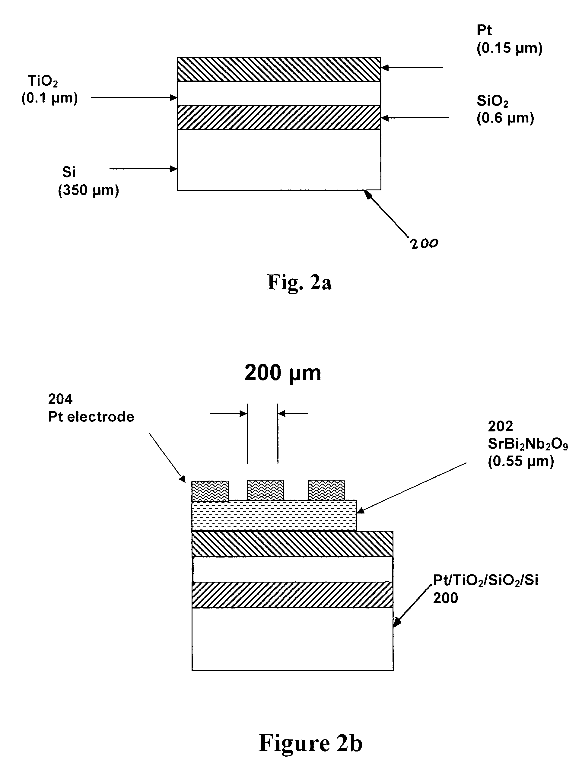
[0023]In accordance with the principles of the invention, one preferred method of fabricating an SrBi2NbO9 (SBN) thin film is described, with reference to FIG. 1. SBN thin films are deposited on Pt / TiO2 / SiO2 / Si substrates using pulsed-laser deposition. An excimer laser having a KrF beam, with a 248 nm wavelength (manufactured by Lamda Physik, model 210i) is used. The laser beam 102 has an energy density of approximately 1.5 J / cm2 and the pulse repetition rate is 10 Hz. The laser beam 102 passes through a mask 104, then through a condensing lens 106 and finally through a quartz window 108 into the deposition chamber 110. The laser beam 102 hits a rotating target 112 to generate a deposition plume 114. The substrate 116 is placed on a rotating heater 118 and is positioned off-axis from the center of the deposition plume 114.

[0024]The SBN is deposited until the thin film grows to 550 nm. A densed ceramic target with 15% excess bismuth was prepared by conventional powder processing. The...


PUM

PropertyMeasurementUnit
Temperatureaaaaaaaaaa
Lengthaaaaaaaaaa

Abstract

SrBi2Nb2O9 (SBN) thin films are deposited on Pt / TiO2 / SiO2 / Si substrates using off-axis pulsed laser deposition technique. Off-axis laser ablation avoids plasma damaging of the surface of SBN thin films and is favorable to grow films along the polarization axis (a–b plane). SBN thin films are grown at 350° C. substrate temperature, with 5 mm away from the plasma focus, and annealed at 750° C. for 1 hour in oxygen ambient. These SBN thin films exhibited giant remnant polarization (Pr) of 50 μC / cm2 with coercive field of 190 kV / cm. The fatigue endurance of these SBN thin films was measured at 400 kV / cm and showed minimal (<20%) polarization degradation of up to 1010 switching cycles. The leakage current density of SBN thin films was found to be about 2×10⁷ up to an applied field of 100 kV / cm. The above-mentioned properties of off-axis deposited SBN thin films, makes it a good material for NVRAM devices.

Description

GOVERNMENT INTERESTS[0001]The claimed invention was made with Government support under grant number INT 0097018 awarded by the National Science Foundation (NSF). The Government has certain rights in this invention.FIELD OF THE INVENTION[0002]The invention relates to thin films which are suitable for use as memory devices, and more specifically to thin films having a giant remnant polarization.BACKGROUND OF THE INVENTION[0003]Ferroelectric materials have been widely studied and applied to the application of non-volatile random access memory (NVRAM), particularly over the last decade. Pb(ZrTi)O3 (PZT) has been one of the leading materials, which exhibits a high value of remnant polarization; it also can be fabricated at relatively low crystallization temperatures. Fatigue (defined as loss of polarization with repeated switching of the field) and imprint are the principle factors limiting commercialization of PZT based NVRAMs. Presently, PZT thin films do not show fatigue resistance ab...

Claims


Application Information

Patent Timeline
IPC IPC(8): B32B9/00B32B15/04
CPCC23C14/08H01L28/55G11C11/16H01L28/65
Inventor KATIYAR, RAM S.BATTACHARYA, PIJUSHDAS, RASMI R.
Owner PUERTO RICO UNIV OF
Why Eureka
Try Eureka