Enhanced high-electron-mobility transistor based on ferroelectric group III nitride polarization reversion

A technology with high electron mobility and polarization reversal, which is applied in circuits, electrical components, semiconductor devices, etc., can solve the problems of no ferroelectric properties and limitations, and achieve low lattice mismatch, film and interface quality Good, growth process compatible effect

Pending Publication Date: 2021-12-03
DALIAN UNIV OF TECH
View PDF0 Cites 0 Cited by
  • Summary
  • Abstract
  • Description
  • Claims
  • Application Information

AI Technical Summary

Problems solved by technology

2DEG can move freely in the two-dimensional space parallel to the heterojunction interface, but it will be strictly restricted in the third dimension, which will lead to the movement of the quantized energy level in the third direction. Therefore, it has excellent electrical properties and has been studied people's attention
However, for a long time, it was believed that the spontaneous polarization of this type of material cannot be reversed by an external electric field, so it does not have ferroelectric properties.

Method used


Image

  • Enhanced high-electron-mobility transistor based on ferroelectric group III nitride polarization reversion
  • Enhanced high-electron-mobility transistor based on ferroelectric group III nitride polarization reversion
  • Enhanced high-electron-mobility transistor based on ferroelectric group III nitride polarization reversion

Examples


Embodiment 1

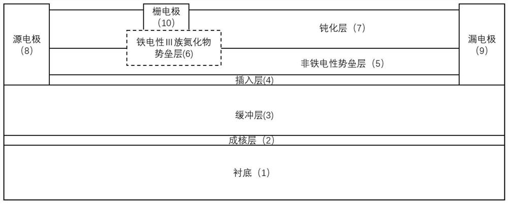
[0032] When the non-ferroelectric barrier layer 5 is omitted, the ferroelectric Group III nitride barrier layer 6 is a complete layer with both ends connected to the source electrode 8 and the drain electrode 9 and covers the insertion layer 4 . The preparation of the device can be realized through the following steps:

[0033] Metal-organic chemical vapor deposition (MOCVD) was used to sequentially deposit an AlN nucleation layer 2 with a thickness of 50 nm, a GaN buffer layer 3 with a thickness of 1.5 μm, an AlN insertion layer 4 with a thickness of 1.5 nm and a thickness of 40 nm on a Si substrate 1. Al 0.64 sc 0.36 N ferroelectric group III nitride barrier layer 6; then use photolithography process and electron beam evaporation process to make source electrode 8 and drain electrode 9; then use electron beam evaporation process to form ferroelectric group III nitride barrier layer 6 Deposit the gate electrode on top, or use photolithography process and electron beam evapo...

Embodiment 2

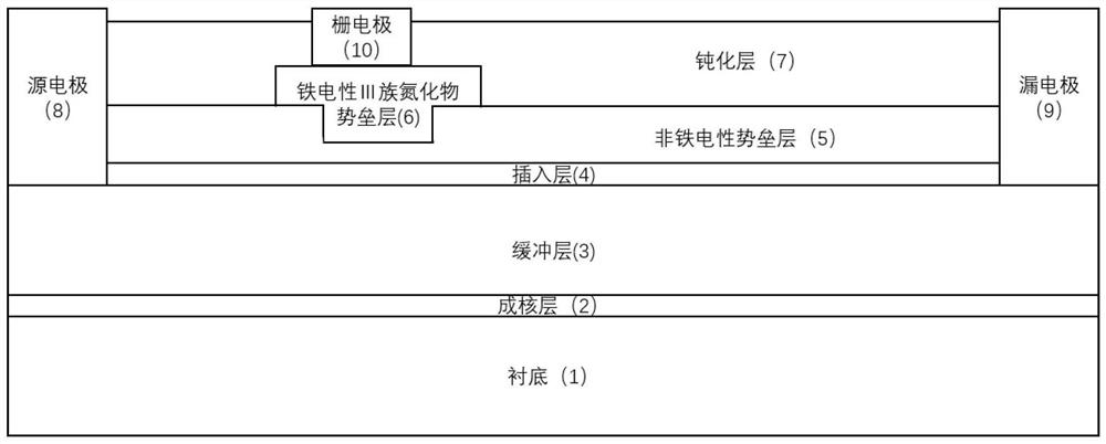
[0035] When the non-ferroelectric barrier layer 5 is not omitted, and the ferroelectric III-nitride barrier layer 6 is partially or completely embedded in the non-ferroelectric barrier layer 5, the device can be prepared by the following steps:

[0036] Metal-organic chemical vapor deposition (MOCVD) was used to sequentially deposit an AlN nucleation layer 2 with a thickness of 60 nm, a GaN buffer layer 3 with a thickness of 2 μm, an AlN insertion layer 4 with a thickness of 1.5 nm, and a GaN layer with a thickness of 30 nm on a Si substrate 1. Al 0.2 Ga 0.8 N non-ferroelectric barrier layer 5; then use photolithography process and electron beam evaporation process to make source electrode 8 and drain electrode 9; then etch groove on barrier layer 5, the groove depth is 20nm, and use molecular Beam epitaxy (MBE) deposits Al with a thickness of 40nm in the etched groove 0.65 sc 0.35 N ferroelectric group III nitride barrier layer 6; then deposit the gate electrode on the fer...

Embodiment 3

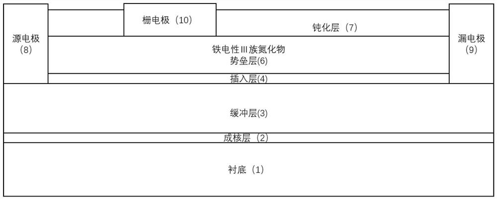
[0038] When the non-ferroelectric barrier layer 5 adopts group III nitrides without ferroelectric properties, and the ferroelectric group III nitride barrier layer 6 is completely embedded in the barrier layer 5, the preparation of the device is realized by the following steps:

[0039] Metal-organic chemical vapor deposition (MOCVD) was used to sequentially deposit an AlN nucleation layer 2 with a thickness of 70 nm, a GaN buffer layer 3 with a thickness of 2.5 μm, an AlN insertion layer 4 with a thickness of 1 nm, and a GaN intercalation layer with a thickness of 30 nm on a sapphire substrate 1. al 0.25 Ga 0.75 N non-ferroelectric barrier layer 5; then use photolithography process and electron beam evaporation process to make source electrode 8 and drain electrode 9; then implant doped modified ions Er, And perform activation diffusion, the diffusion depth is 20nm, so that the non-ferroelectric barrier layer 5 in this part of the region has ferroelectric properties, and the...


PUM

PropertyMeasurementUnit
Thicknessaaaaaaaaaa
Thicknessaaaaaaaaaa
Thicknessaaaaaaaaaa

Abstract

;An enhanced high-electron-mobility transistor based on ferroelectric III nitride polarization reversion comprises a substrate, a nucleating layer, a buffer layer, an insertion layer, a barrier layer and a passivation layer in sequence from bottom to top and the barrier layer comprises a non-ferroelectric barrier layer and a ferroelectric group III nitride barrier layer, and the ferroelectric group III nitride barrier layer is arranged between the non-ferroelectric barrier layer and the passivation layer. The buffer layer and the barrier layer form heterojunctions with different forbidden band widths, and the forbidden band width of the buffer layer is smaller than the forbidden band width of the barrier layer; two ends of the upper surface of the buffer layer are provided with a source electrode and a drain electrode; and a gate electrode is arranged on the ferroelectric III nitride barrier layer, and the gate electrode is nested in the passivation layer. The buffer layer and the barrier layer are made of III-V group semiconductor materials, the preparation processes of the buffer layer and the barrier layer are compatible, the film growth quality of each layer is high, and the interface characteristic between the films is good; and meanwhile, the ferroelectric hysteresis loop rectangularity of the group III nitride ferroelectric material is high, the remanent polarization intensity is high, the retention time of the closed and on states of the device is long, and the service reliability is higher.

Description

technical field [0001] The invention belongs to the field of semiconductor devices, and relates to a class of enhanced high electron mobility transistor devices that utilize the polarization reversal characteristics of ferroelectric Group III nitrides to realize the off state under zero bias voltage of the gate, and can modulate the conduction of the device at the same time. The concentration of the two-dimensional electron gas in the heterojunction interface channel in the state. Background technique [0002] The group III nitride wide bandgap semiconductor material system, including GaN, AlN, BN and their multi-component alloys, is a new type of semiconductor material that has received great attention in recent years. Compared with the first-generation and second-generation semiconductor materials such as silicon, germanium and gallium arsenide, group III nitride semiconductor materials have excellent properties such as high critical breakdown electric field strength, high...

Claims


Application Information

Patent Timeline
IPC IPC(8): H01L29/778
CPCH01L29/7786
Inventor 周大雨隋金洋孙纳纳习娟
Owner DALIAN UNIV OF TECH
Why Eureka
Try Eureka