Semiconductor device and method for producing the same

a technology of semiconductors and dielectric films, applied in semiconductor devices, electrical equipment, transistors, etc., can solve the problems of increasing the leak current of the gate through the resultant crystal grain boundaries or defect level, increasing the leak current of the gate, and insufficient thermal stability of the conventional high-k gate insulating film

Inactive Publication Date: 2007-01-02
PANASONIC SEMICON SOLUTIONS CO LTD
View PDF16 Cites 21 Cited by
  • Summary
  • Abstract
  • Description
  • Claims
  • Application Information

AI Technical Summary

Benefits of technology

[0058]This allows the defects in the high-k gate insulating film having t

Problems solved by technology

When the thickness of a gate insulating film is being reduced to achieve the miniaturization, problems such as an increase of a gate leak current due to tunneling current are caused.
However, in the conventional high-k gate insulating film, when heat history is applied by a high temperature treatment during the production p

Method used


Image

  • Semiconductor device and method for producing the same
  • Semiconductor device and method for producing the same
  • Semiconductor device and method for producing the same

Examples


first embodiment

[0073]Hereinafter, a semiconductor device of a first embodiment of the present invention, more specifically, a MISFET will be described with reference to the accompanying drawings.

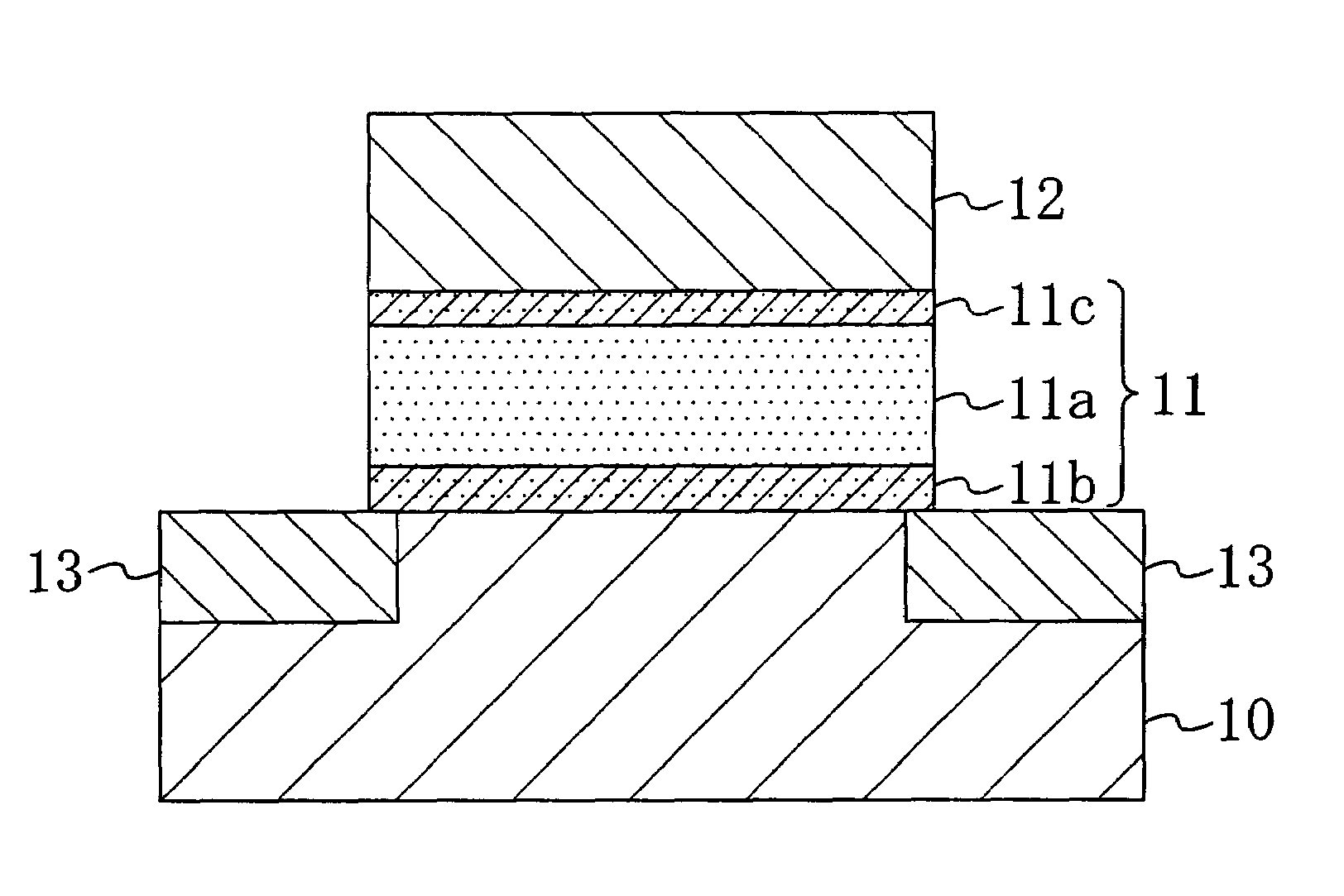
[0074]FIG. 1 shows the cross-sectional structure of a semiconductor device of a first embodiment.

[0075]As shown in FIG. 1, a gate electrode 12 is formed on a silicon substrate 10 via a gate insulating film 11. An impurity diffusion layer 13 serving as a source region or a drain region is formed on both sides of the gate electrode 12 in the silicon substrate 10. The gate insulating film 11 includes a high dielectric constant film 11a made of insulative metal oxide, a lower barrier film 11b formed below the high dielectric constant film 11a, and an upper barrier film 11c formed above the high dielectric constant film 11a.

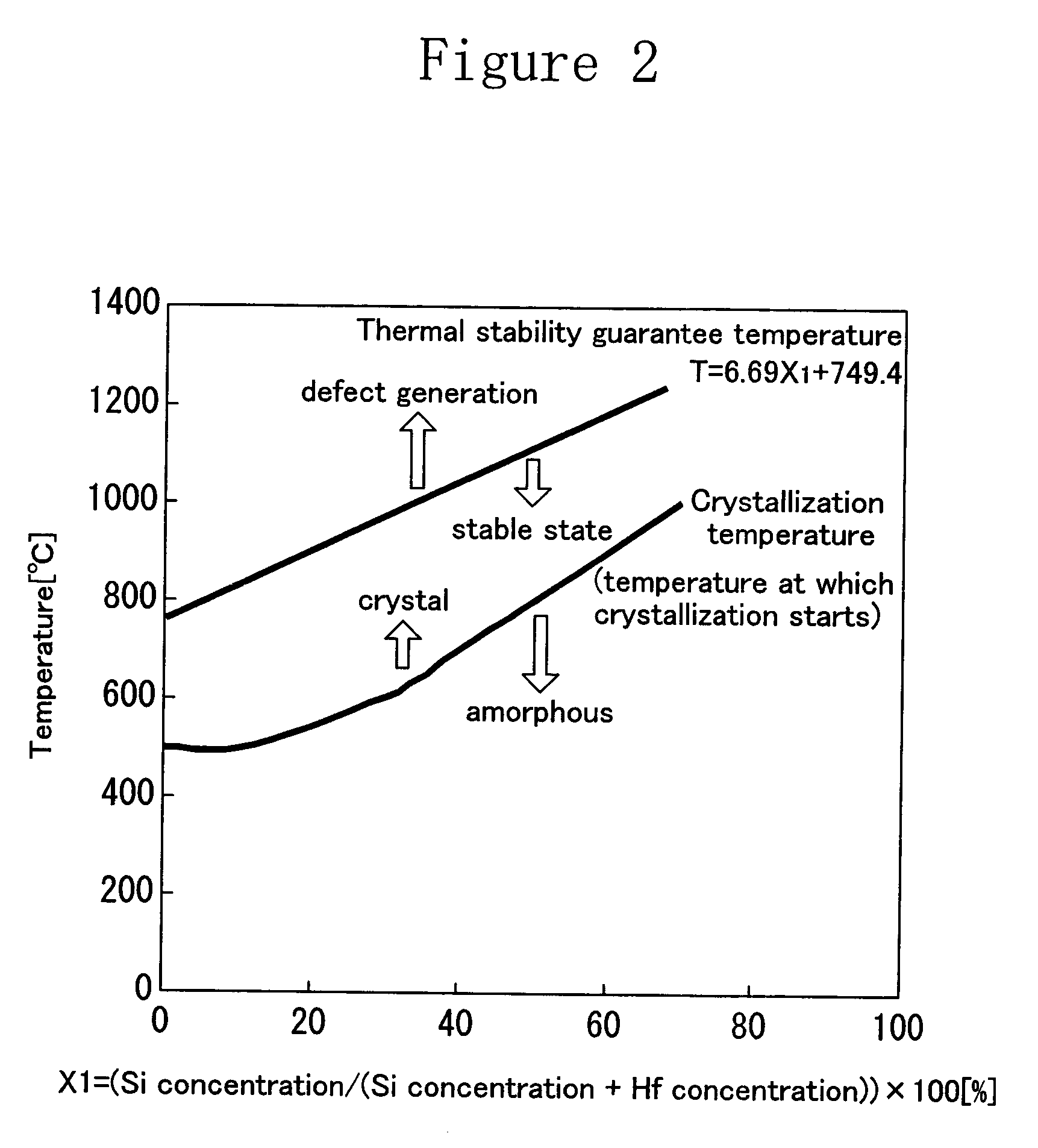
[0076]More specifically, the high dielectric constant film 11a is formed of a substance in which silicon is contained in hafnium oxide (HfO2) having a high relative dielectric constant, tha...

second embodiment

[0107]Hereinafter, a method for producing a semiconductor device of a second embodiment of the present invention, specifically, a method for producing a MISFET will be described with reference to the accompanying drawings.

[0108]FIGS. 7A to 7C and 8A to 8C are cross-sectional views showing the processes of a method for producing a semiconductor device of the second embodiment.

[0109]First, as shown in FIG. 7A, an insulating film for isolation (not shown) is formed on a p-type silicon (100) substrate 20, and a device forming region is segmented. Then, standard RCA cleaning and diluted HF cleaning are performed with respect to the surface of the silicon substrate 20. Thereafter, a silicon nitride film (Si3N4 film) 21A having a thickness of about 0.7 nm is formed on the silicon substrate 20 with NH3 gas at a temperature of about 700° C. In this process, sufficient hydrogen is captured in the Si3N4 film 21A. The Si3N4 film 21A eventually becomes the lower barrier film 21 (see FIG. 7C).

[01...


PUM


Abstract

A gate electrode is formed on a substrate via a gate insulating film. The gate insulating film includes a high dielectric constant film containing a metal, oxygen and hydrogen, and a lower barrier film formed below the high dielectric constant film and containing a metal, oxygen, silicon and nitrogen.

Description

RELATED APPLICATIONS[0001]This application is a divisional of application Ser. No. 10 / 122,366 filed Apr. 16, 2002 now U.S. Pat. No. 6,642,131.[0002]This application claims priority from U.S. Provisional Application No. 60 / 299,478, filed on Jun. 21, 2001, and Japanese Patent Application No. 2001-395734, filed Dec. 27, 2001.BACKGROUND OF THE INVENTION[0003]The present invention relates to a semiconductor device and a method for producing the same, in particular, a high dielectric constant film used for a gate insulating film.[0004]With recent technological advance with respect to high integration and high speed in semiconductor devices, miniaturization of MOSFETs has been under development. When the thickness of a gate insulating film is being reduced to achieve the miniaturization, problems such as an increase of a gate leak current due to tunneling current are caused. In order to suppress this problem, there has been research on an approach to increase a physical thickness while rea...

Claims


Application Information

Patent Timeline
IPC IPC(8): H01L21/8238H01L29/96H01L21/28H01L29/51
CPCH01L21/28176H01L21/28185H01L21/28194H01L29/518H01L29/513H01L29/516H01L29/517H01L21/28202
Inventor HARADA, YOSHINAO
Owner PANASONIC SEMICON SOLUTIONS CO LTD
Why Eureka
Try Eureka