Inversion bit line, charge trapping non-volatile memory and method of operating same

a non-volatile memory and bit line technology, applied in the field of electric programmable and erasable, non-volatile memory, can solve the problems of large threshold voltage vt distribution of erase, poor charge retention, large threshold voltage vt distribution, etc., and achieve low current high-speed programming and easy scaling

Active Publication Date: 2007-01-02
MACRONIX INT CO LTD
View PDF76 Cites 52 Cited by
  • Summary
  • Abstract
  • Description
  • Claims
  • Application Information

AI Technical Summary

Benefits of technology

[0009]An inversion bit line charge trapping memory cell is described which has no implanted source and drain bit lines. Rather, a field induced inversion layer is used to replace the source and drain implants. As a result the memory cell is more easily scaled to smaller dimensions. Embodiments of the memory cell are adapted to store two bits, one on the left side and one on the right side of the charge trapping structure. A positive threshold voltage erase state is described for embodiments of the memory cell using negative gate voltage Fowler Nordheim FN tunneling which establishes a charge balance condition at a positive voltage, permitting over-erase problems. A low current, source side, hot electron injection programming method is described for embodiments of the memory cell, which is suitable for use with inversion bit lines, and achieves low current high-speed programming for both left and right side of the memory cells.
[0012]The charged balance state for embodiments of the memory cell achieved by the erase process results in a target low threshold voltage that is positive, and greater than two volts in some embodiments, and more preferably greater than three volts and other embodiments. The memory cells are engineered in some embodiments to adjust the magnitude of the target low threshold voltage. For example, relatively high work function materials, such as p-type polysilicon, can be used as the control gates in order to reduce the magnitude of the charged balanced state.
[0027]Memory technology described herein achieves significant advantages over the prior art. The memory is easy to scale to smaller minimum dimensions than conventional charge trapping memory cells or cells based on floating gate technology because of the elimination of buried source and drained diffusion regions. The cell size can be very small because problems with punch-through that arise with diffusion source and drain regions are eliminated. Programming speed is faster than conventional charge trapping memory cells in embodiments of the technology that use inversion bit line induced low current source side injection. The erase algorithm in embodiments of the technology described is simple and fast, implementing a positive erase threshold state. Memory technology described herein supports two bits per cell for high-density arrays. Furthermore, the memory technology avoids problems with data retention that arise in prior art charge trapping structures that generate hot holes during operation.

Problems solved by technology

Although the erase speed is fast using this technique, the charge retention is poor due to the charge leakage through ultra-thin bottom oxide.
However, the hot hole injection causes oxide damage, leading to charge loss in the high threshold cell and charge gain in the low threshold cell.
This difference in erase speed results in a large threshold voltage Vt distribution of the erase state, where some of the cells become hard to erase and some of them are over-erased.
Thus the target Vt window is closed after many program and erase cycles and poor endurance is observed.
This phenomenon will become more serious when the technology keeps scaling down.
One limitation on the size of traditional memory cells arises from the use of diffusion lines in semiconductor substrates for source and drain terminals.
The diffusion of impurities used to form the diffusion lines spreads out slightly beyond the locations in which the implant is made, increasing the size of the diffusion region, and making it difficult to shrink to smaller and smaller minimum dimensions, and causing other limitations on cell size, including minimum channel lengths for prevention of punch-through.
However, practical implementations of inversion bit line based memory devices have not been reported in the literature, based on charge trapping memory cells.

Method used


Image

  • Inversion bit line, charge trapping non-volatile memory and method of operating same
  • Inversion bit line, charge trapping non-volatile memory and method of operating same
  • Inversion bit line, charge trapping non-volatile memory and method of operating same

Examples


Embodiment Construction

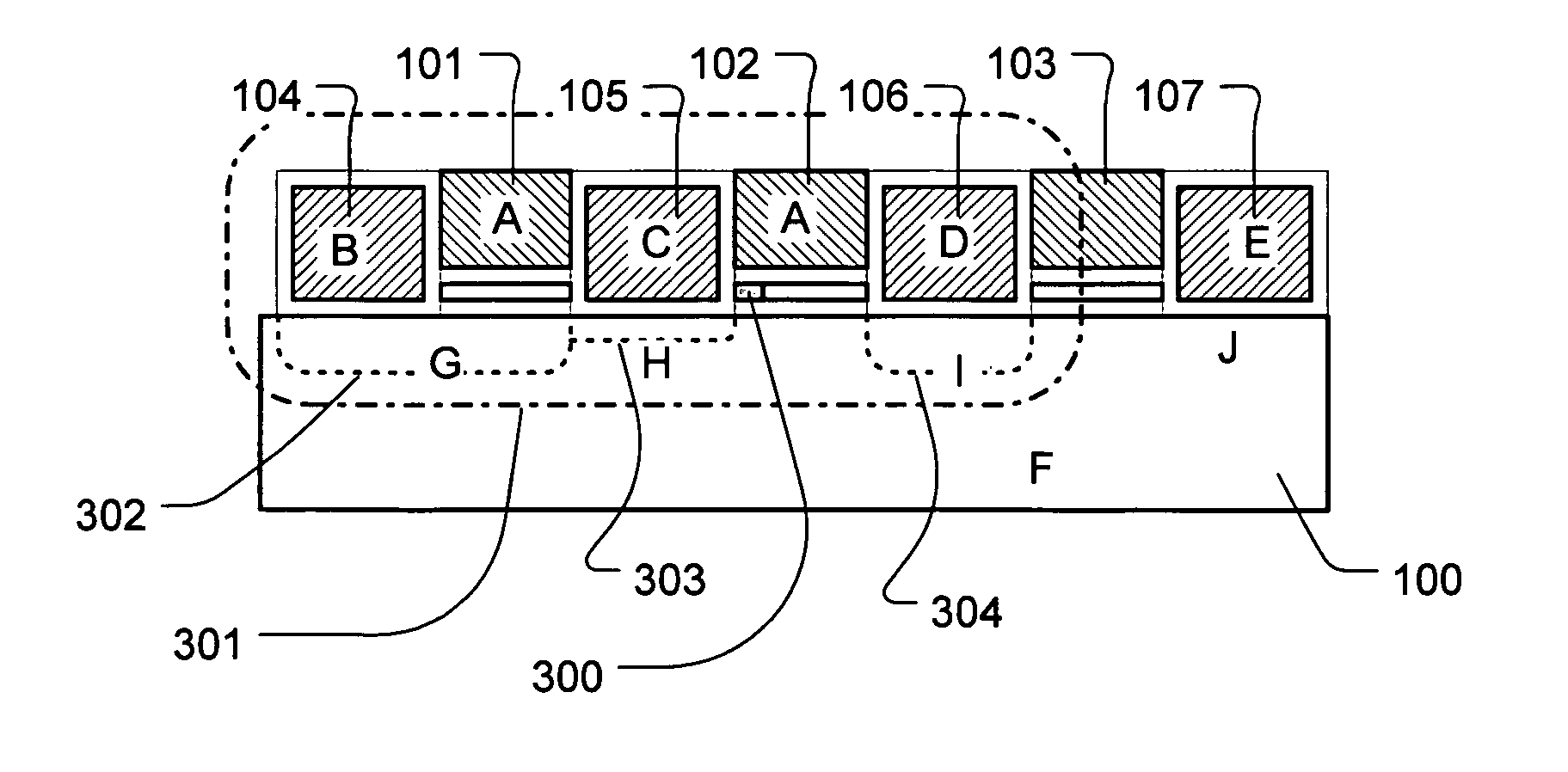
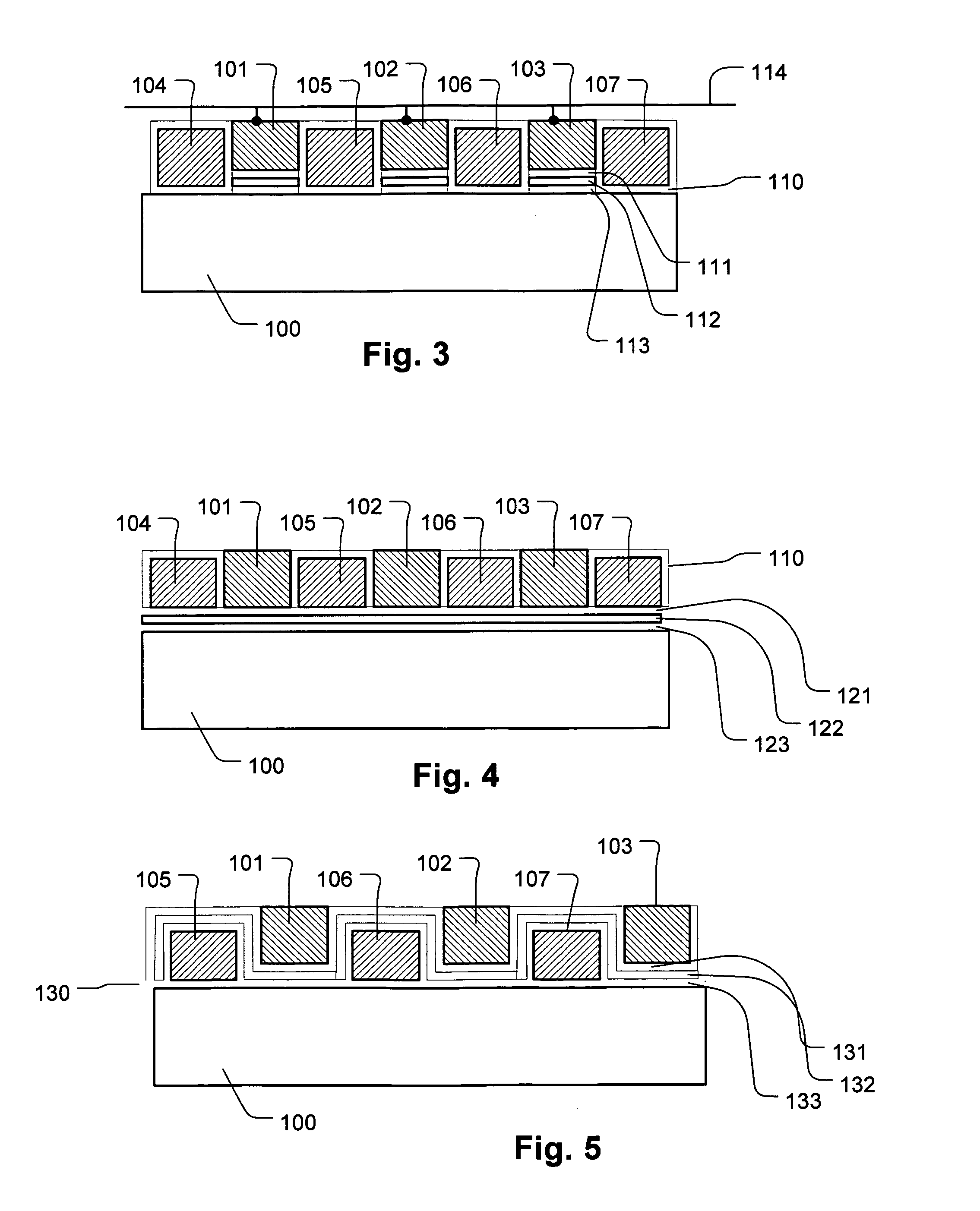
[0045]A detailed description of embodiments of the present invention is provided with reference to the FIGS. 1–16.

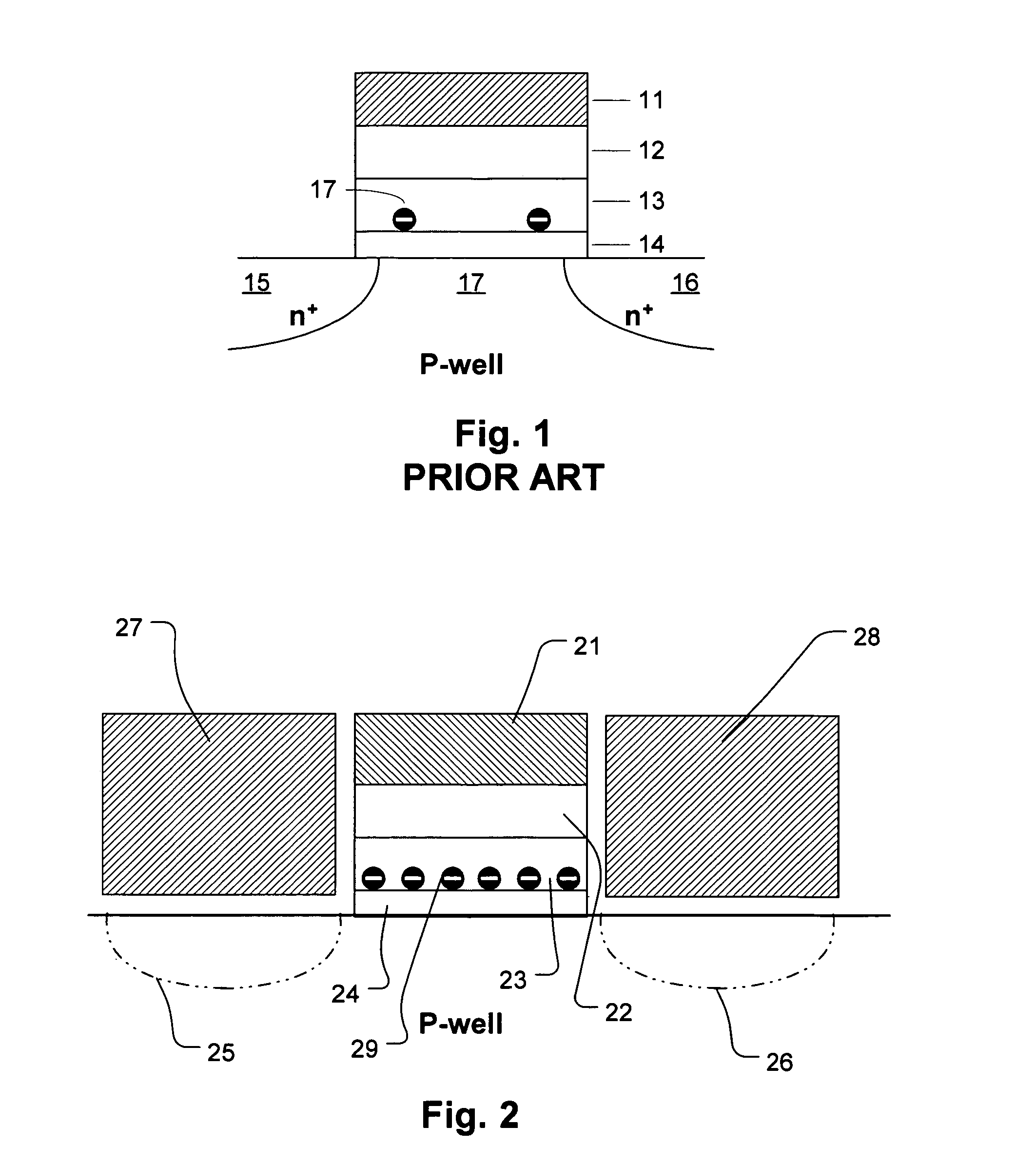
[0046]FIG. 1 is a simplified diagram of a charge trapping memory cell of the prior art. The substrate includes n+ doped regions 15 and 16, and a p-doped region 17 between the n+ doped regions 15 and 16. The n+ doped regions 15 and 16 provide diffusion lines that act as source and drain terminals. The remainder of the memory cell includes a charge trapping structure including a bottom dielectric 14 on the substrate, a charge trapping layer 13 on the bottom dielectric 14 (bottom oxide), a top dielectric 12 (top oxide) on the charge trapping layer 13, and a control gate 11 on the top dielectric 12. Typically, the control gate 11 comprises n-type polysilicon, and is coupled to a word line (not shown). The charge trapping structure has trapped charge in the charge trapping layer 13 such as represented by electron 17. Typically, such cells are erased by band-to-band tunneling ...


PUM


Abstract

A charge trapping memory device in which a field induced inversion layer is used to replace the source and drain implants. The memory cell are adapted to store two bits, one on the left side and one on the right side of the charge trapping structure. A positive threshold voltage erase state is induced using negative gate voltage Fowler Nordheim FN tunneling which establishes a charge balance condition at a positive voltage. A low current, source side, hot electron injection programming method is used.

Description

BACKGROUND OF THE INVENTION[0001]1. Field of the Invention[0002]The present invention relates to electrically programmable and erasable, nonvolatile memory, and more particularly to such memory based on charge trapping memory cells.[0003]2. Description of Related Art[0004]Electrically programmable and erasable non-volatile memory technologies based on charge storage structures known as EEPROM and flash memory are used in a variety of modern applications. A number of memory cell structures are used for EEPROM and flash memory. As the dimensions of integrated circuits shrink, greater interest is arising for memory cell structures based on charge trapping dielectric layers, because of the scalability and simplicity of the manufacturing processes. Memory cell structures based on charge trapping dielectric layers include structures known by the industry names NROM, SONOS, and PHINES, for example. These memory cell structures store data by trapping charge in a charge trapping dielectric l...

Claims


Application Information

Patent Timeline
Patent Type & Authority Patents(United States)
IPC IPC(8): G11C11/34
CPCG11C16/0475
Inventor LUNG, HSIANG LAN
Owner MACRONIX INT CO LTD
Why Eureka
Try Eureka