Forming system for insulation film
- Summary
- Abstract
- Description
- Claims
- Application Information
AI Technical Summary
Benefits of technology
Problems solved by technology
Method used
Image

Examples
Embodiment Construction
[0047]The forming method of the insulation film according to the embodiment of the present invention will be described referring to the drawings.
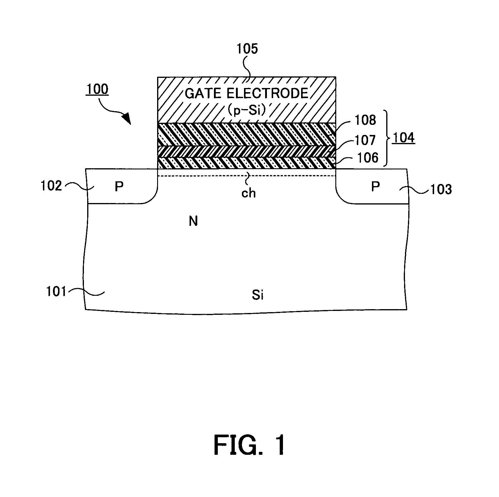
[0048]The insulation film, formed according to the embodiment of the present invention, comprises a gate insulator of a Metal Insulator Semiconductor Field Effect Transistor (MISFET) shown in FIG. 1.
[0049]As shown in FIG. 1, MISFET 100 comprises, a P-type drain region 102 and source region 103 in the surface region of an N-type silicon substrate 101, a gate insulator 104 formed on the surface region (channel region) of the silicon substrate 101, which is placed between the P-type drain region 102 and source region 103, and a gate electrode 105 formed on the gate insulator 104. Drain region 102 and source region 103, are respectively connected to a drain electrode and source electrode, comprising a MISFET 100. Silicon substrate 101, drain region 102 and source region 103, respectively may be opposite conductivity types.
[0050]On the silicon s...
PUM
| Property | Measurement | Unit |
|---|---|---|
| Thickness | aaaaa | aaaaa |
| Thickness | aaaaa | aaaaa |
| Thickness | aaaaa | aaaaa |
Abstract
Description
Claims
Application Information