
Semiconductor optical amplifier suitable for coarse WDM communications and light amplification method

a technology of optical amplifier and semiconductor, applied in the structure of semiconductor amplifier, semiconductor laser, laser, etc., can solve the problem that the semiconductor optical amplifier is difficult to be used as a broadband optical amplifier, and achieve the effect of suppressing gain saturation, reducing gain difference, and constant gain

Inactive Publication Date: 2007-01-23
FUJITSU LTD
View PDF24 Cites 8 Cited by
  • Summary
  • Abstract
  • Description
  • Claims
  • Application Information

AI Technical Summary

Benefits of technology

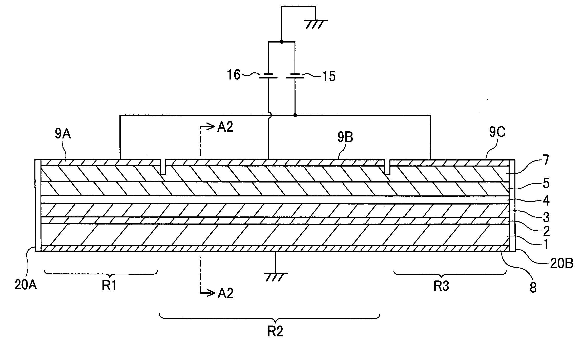
[0012]With this configuration, it is possible to reduce a gain difference between two transition wavelength ranges.
[0014]Sections at the same current linear density are disposed dispersively. The length of each section can therefore be made short. It is possible to prevent light in a specific wavelength range from being excessively amplified so that gain saturation can be suppressed.
[0016]With this method, it is possible to reduce a gain difference between two transition wavelength ranges.

Problems solved by technology

This semiconductor optical amplifier is difficult to be used as a broadband optical amplifier used in coarse WDM.

Method used


Image

  • Semiconductor optical amplifier suitable for coarse WDM communications and light amplification method
  • Semiconductor optical amplifier suitable for coarse WDM communications and light amplification method
  • Semiconductor optical amplifier suitable for coarse WDM communications and light amplification method

Examples


first embodiment

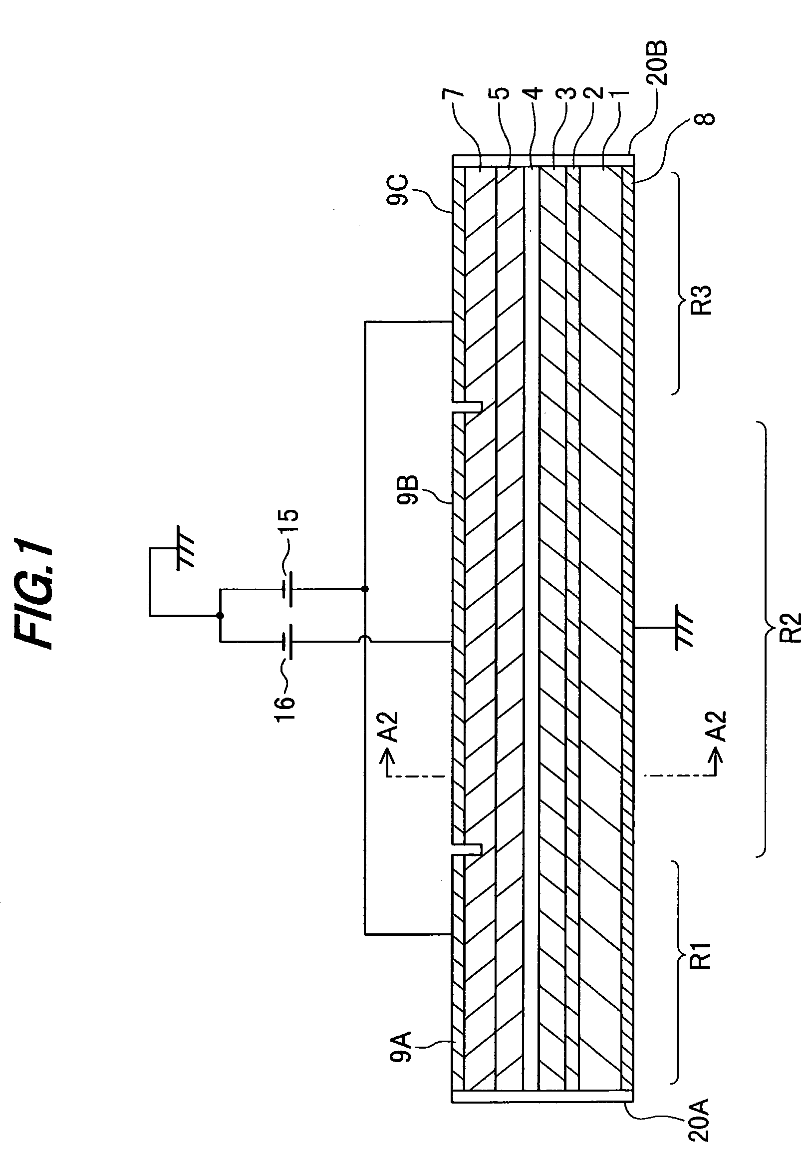
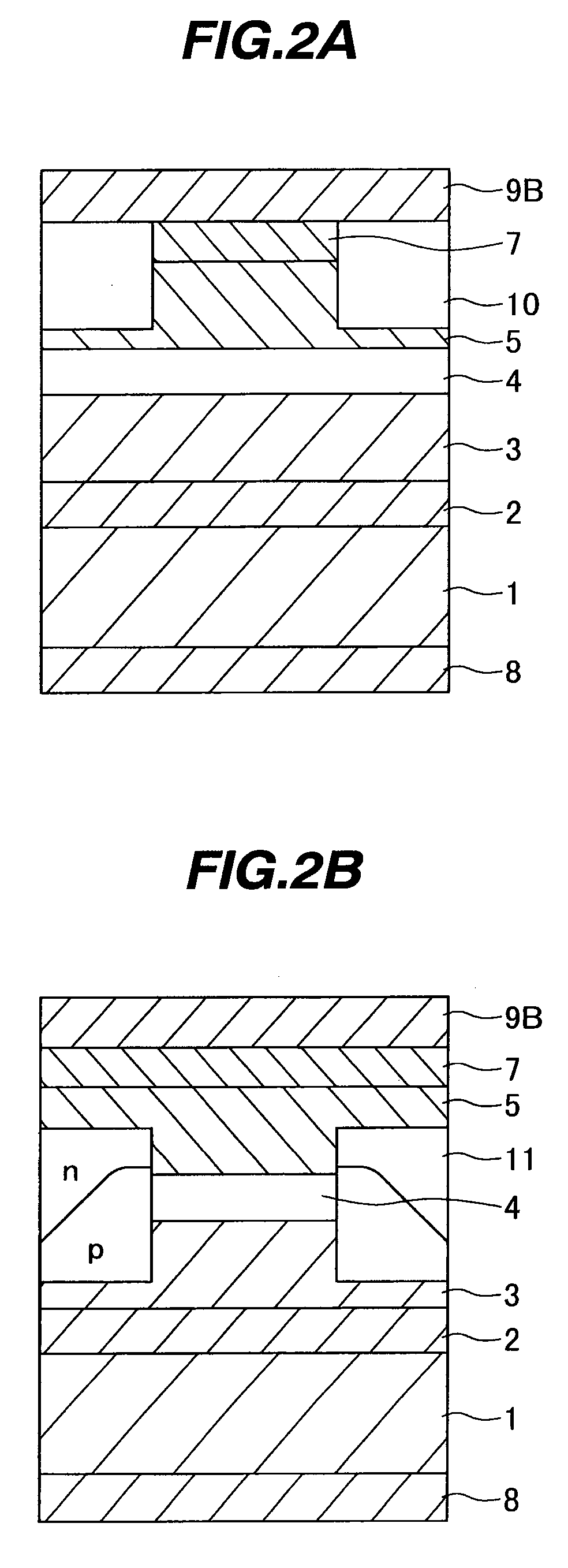
[0047]FIG. 1 is a cross sectional view of a semiconductor optical amplifier of the first embodiment as viewed along a direction parallel to the light propagation direction. On a substrate 1 made of n-type InP, a buffer layer 2 made of n-type InP and having a thickness of 100 to 200 nm is epitaxially grown. The buffer layer 2 is used for providing an underlayer surface having good crystallinity. If the crystallinity of the substrate 1 is good, the butter layer 2 may be omitted. On the buffer layer 2, a clad layer 3 is formed which is made of n-type InP and has a thickness of 3 μm. The n-type impurity concentration of each of the substrate 1, buffer layer 2 and clad layer 3 is 1×10 18 cm−3 for example.

[0048]On the clad layer 3, an active layer 4 of 0.5 μm in thickness is formed. The active layer 4 contains quantum dots having a tensile strain. The structure of the active layer 4 will be later described.

[0049]On the active layer 4, a clad layer 5 of p-type InP is epitaxially grown to a...

second embodiment

[0090]It can be seen from the comparison of FIG. 10 with FIG. 6 that the light intensity in the wavelength range from 1100 to 1200 nm is weak. In the second embodiment, because each of the regions having a high current linear density (e.g., regions R11, R13, . . . ) is short, the light intensity does not rise too high even if light in the wavelength range from 1100 to 1200 nm is amplified in the regions having the high current linear density. It is therefore possible to prevent light in the wavelength range from 1100 to 1200 nm from being amplified excessively. If light in the wavelength range from 1100 to 1200 nm is amplified too much, gain saturation occurs.

[0091]As seen from FIG. 9, the gain coefficient in the regions R11 to R19 is generally constant along the light propagation direction (vertical direction in FIG. 9). Namely, there is no gain saturation. This is because light amplification is suppressed in the wavelength range from 1100 to 1200 nm.

[0092]FIG. 11A shows the relati...


PUM


Abstract

An active layer contains quantum structures. The active layer amplifies light propagating therein while current is injected therein. Electrodes are provided for sections of the active layer sectionalized along a light propagation direction. The electrodes inject different currents into the sections. Current is supplied to the electrodes in such a manner that a first current density is set to one section of the active layer and a second current density is set to another section. The first current density is lower than that at a cross point and the second current density is higher than that at the cross point. The cross point is a cross point between gain coefficient curves at least two different transition wavelengths of the quantum structures. The curves are drawn in a graph showing a relation between a density of current injected into the active layer and a gain coefficient of the active layer.

Description

CROSS REFERENCE TO RELATED APPLICATIONS[0001]This application is based on and claims priority of Japanese Patent Application No. 2003-76893 filed on Mar. 20, 2003, the entire contents of which are incorporated herein by reference.BACKGROUND OF THE INVENTION[0002]A) Field of the Invention[0003]The present invention relates to a semiconductor optical amplifier and a light amplification method, and more particularly to a semiconductor optical amplifier which induces optical amplification upon flowing current and introducing light into an active layer containing quantum dots, quantum wires or quantum dashes and to a light amplification method.[0004]B) Description of the Related Art[0005]For the cost reduction of metro optical networks and access optical networks, it is expected that coarse Wavelength Division Multiplexing (WDM) having a wide inter-channel wavelength (about 20 nm) will be widely used. Coarse WDM does not require precise control over the wavelengths of light sources and f...

Claims


Application Information

Patent Timeline
IPC IPC(8): H01S3/00H01S5/00H01S5/042H01S5/0625H01S5/10H01S5/34H01S5/50
CPCB82Y20/00H01S5/50H01S5/0425H01S5/0625H01S5/1053H01S5/06812H01S5/34H01S5/341H01S5/3412H01S5/1096H01S5/5027H01S5/04256H01S2301/02
Inventor AKIYAMA, TOMOYUKI
Owner FUJITSU LTD
Learn More