Washing liquid for semiconductor substrate and method of producing semiconductor device

Active Publication Date: 2007-02-13
DONGWOO FINE CHEM CO LTD
View PDF13 Cites 5 Cited by
  • Summary
  • Abstract
  • Description
  • Claims
  • Application Information

AI Technical Summary

Problems solved by technology

Since it is also necessary that an insulation membrane is formed on the surface of the copper wiring, after a copper wiring is formed by CMP, and washing with washing liquid is conducted, there is a problem that an organic substance due to an additive contained in washing liquid remains and poor adherence occurs between the copper wiring and insulation membrane.

Method used


Image

  • Washing liquid for semiconductor substrate and method of producing semiconductor device
  • Washing liquid for semiconductor substrate and method of producing semiconductor device

Examples


example 6

[0045]Washing liquid of a composition shown in Table 1 was prepared. In this washing liquid, a silicon wafer on which a 4000 Å copper (Cu) membrane had been formed by a plating method was immersed as a test piece at 40° C. for 5 minutes, then, rinsed in ultra pure water for 30 seconds. The amount of residual carbon on the surface of the sample before and after washing treatment was measured by an X-ray excitation photoelectron spectral apparatus. The residual carbon amounts were relatively compared by measuring the ratio of photoelectron strength derived from Cu membrane to photoelectron strength derived from carbon (C) on the surface. The residual carbon amount C / Cu on the surface of copper before conducting washing treatment was 1.19. The results are shown in Table 2. As shown in Table 2, washing liquid composed of tetramethylammonium hydroxide and mannitol shows approximately the same level of residual carbon after washing as that before washing.

[0046]

TABLE 1ComparativeExampleexa...

example 7

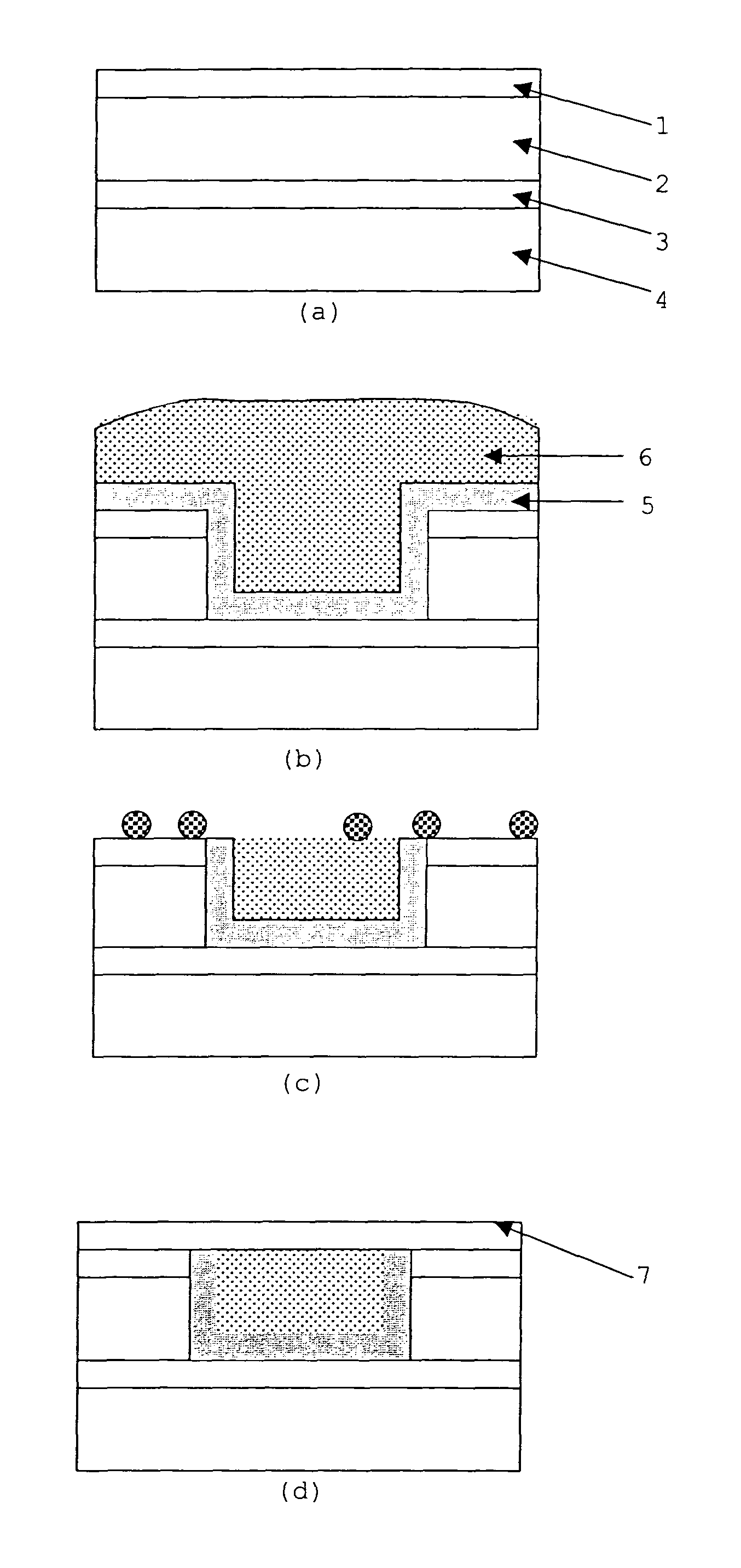
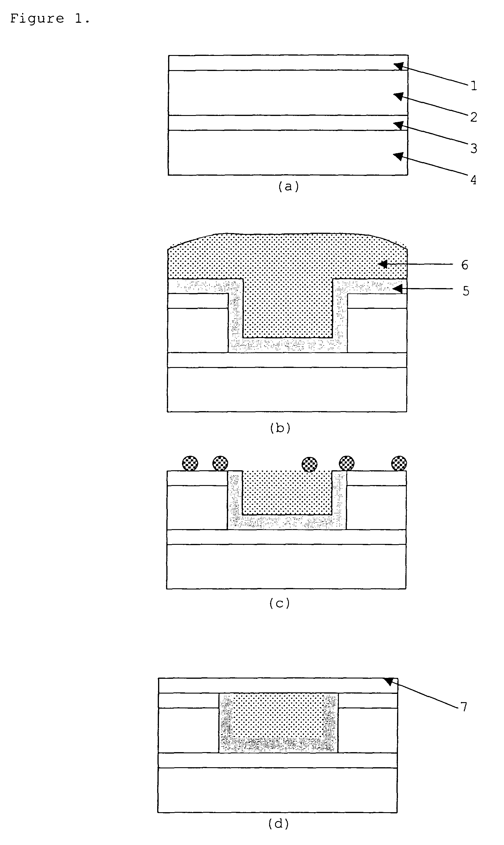
[0048]A semiconductor substrate for copper wiring having a structure shown in FIG. 1(b) was polished by a CMP polishing apparatus and a known polishing agent containing grinding grains made of silica, then, immersed in the washing liquid shown in Example 6 at 40° C. for 2 minutes, to effect washing thereof. During washing, irradiation with ultrasonic wave having a frequency of 950 kHz was used together.

[0049]Then, the surface of the copper wiring was observed by an electron microscope, as a result, silica grinding grains and the like significantly adhered before washing were removed completely, and etching and corrosion were not observed at all on the surface of the copper wiring.

[0050]According to the present invention, it is possible to provide washing liquid for semiconductor substrate removing polishing agent grains of silica, alumina or the like and polishing trashes of copper and the like generated by polishing and showing little residual organic substances after washing, whil...


PUM

PropertyMeasurementUnit
Percent by massaaaaaaaaaa
Concentrationaaaaaaaaaa

Abstract

An object of the present invention is to provide washing liquid for semiconductor substrate capable of removing grinding grains of silica, alumina or the like in a polishing agent and polishing trashes of copper, and capable of leaving little organic substance due to an additive used for preventing corrosion of copper on the surface of a copper wiring after washing, while corrosion of copper is suppressed, and a method of producing a semiconductor device using this washing liquid. The object is achieved by washing liquid for a semiconductor substrate having a copper wiring, comprising a basic compound and at least one selected from the group consisting of sugar alcohols and saccharides. Also the present invention provides a method of producing a semiconductor device comprising a step of forming a copper wiring by chemical mechanical polishing and washing it with washing liquid for a semiconductor substrate containing a basic compound and at least one selected from the group consisting of sugar alcohols and saccharides.

Description

FIELD OF THE INVENTION[0001]The present invention relates to washing liquid for a semiconductor substrate having a copper wiring and the method of producing a semiconductor device.BACKGROUND OF THE INVENTION[0002]Recently, various materials are being developed for high integration and high performance of semiconductor devices. As the wiring materials in devices, aluminum and its alloys are used conventionally.[0003]An aluminum wiring is formed by patterning with a photoresist on an aluminum membrane formed on an insulation membrane, etching, and then, peeling the masked photoresist. Therefore, on the surface of the aluminum wiring, there is significant adhesion of the photoresist not peeled, and there are the residue of the photoresist ashed by oxygen plasma and the like during etching, and gas components used in patterning and plasma treating, on the side surface of the aluminum wiring, bottom between the wiring and wiring, top of the wiring, and the like.[0004]For removing these r...

Claims


Application Information

Patent Timeline
IPC IPC(8): C11D1/62H01L21/304C11D3/22C11D7/06C11D11/00C23G1/24H01L21/02H01L21/306H01L21/321H01L21/3213
CPCC11D3/221C11D7/06H01L21/02074C23G1/24C11D11/0047C11D2111/22H01L21/304
Inventor TAKASHIMA, MASAYUKI
Owner DONGWOO FINE CHEM CO LTD
Why Eureka
Try Eureka