

High resolution analytical probe station
a probe station and high-resolution technology, applied in the direction of fault location by increasing the destruction of the fault, semiconductor/solid-state device testing/measurement, instruments, etc., can solve the problem that modern structures have now reached a size that no longer allows viewing with standard light microscopes, and achieve the effect of improving low-current testing accuracy, reducing the risk of electrical shock, and preventing interferen
- Summary
- Abstract
- Description
- Claims
- Application Information
AI Technical Summary
Benefits of technology
Problems solved by technology
Method used
Image

Examples
Embodiment Construction
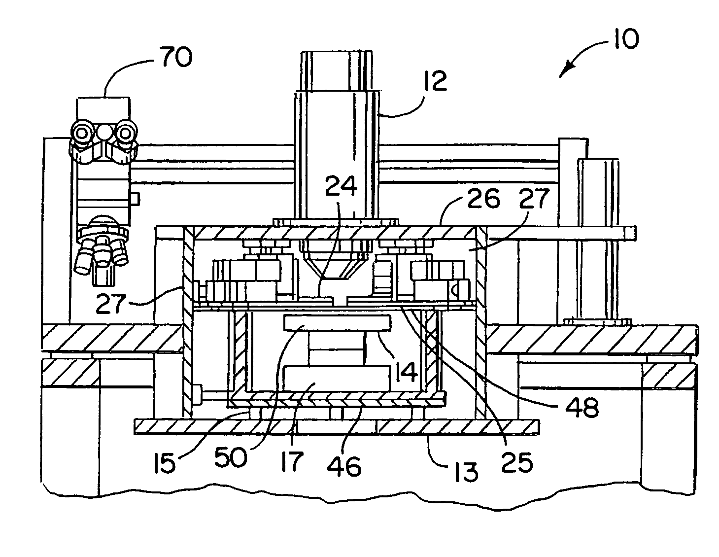
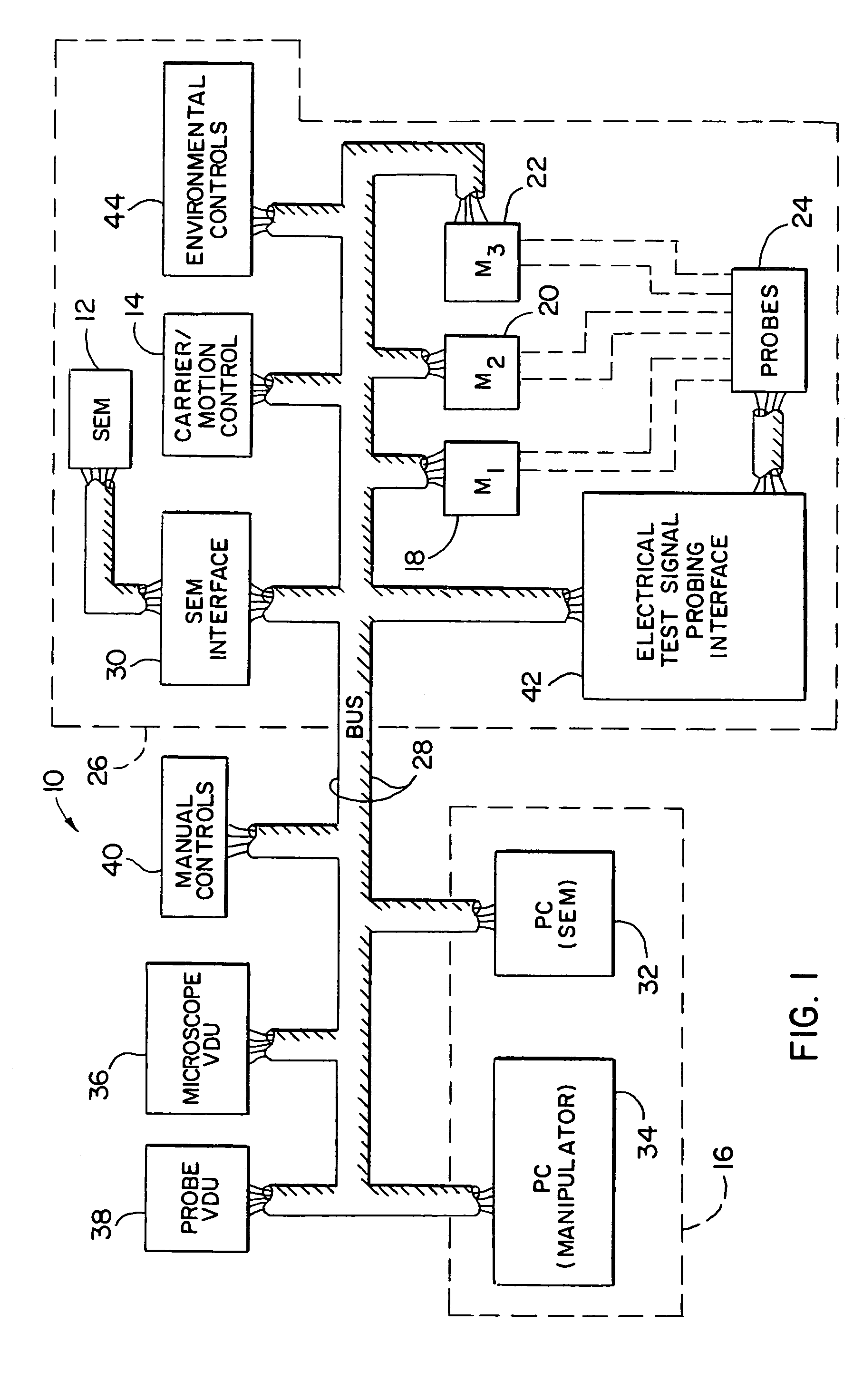
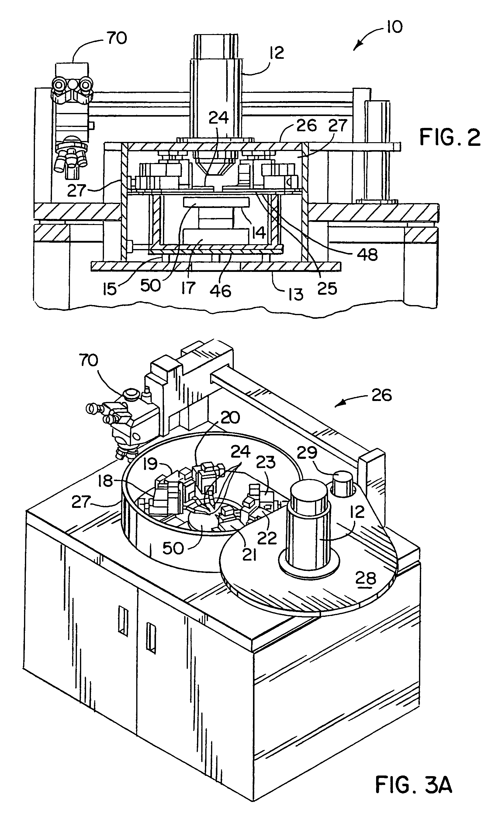
[0049]Referring to the drawings and especially to FIGS. 1 and 2, a system 10 is shown for high resolution analytical probing of an integrated circuit specimen, (e.g., a semiconductor wafer 50). The system 10 is capable of applying electrical test signals to an integrated circuit specimen 50, which may include whole wafers, packaged parts, or wafer fragments. Thus the system 10 may probe entire wafers in addition to a large variety of similarly sized specimens. A conventional scanning electron microscope (SEM), an X-ray microscope for material analysis during probing functions, or a Focus Ion Beam (FIB) system 12, may be employed for enhanced capabilities. Thus, the prober may be integrated into FIB systems as well as SEM systems. The embodiment described herein uses a SEM provided by R.J. Lee Instruments Ltd. which is positioned for observing a surface of the specimen 50 exposing electrically conductive terminals on the specimen 50. See, e.g., FIG. 4, discussed below. The system 10 ...
PUM
 Abstract
Description
Claims
Application Information