Optical active device

a technology of optical active devices and optical elements, applied in the field of optical active devices, can solve the problems of large loss due to imperfect production precision in each boundary surface between the refractive index periodic structure, the specific mode selection between respective modes, and the weak theory of the photonic crystal

Inactive Publication Date: 2007-02-20
MITSUBISHI ELECTRIC CORP +1
View PDF17 Cites 20 Cited by
  • Summary
  • Abstract
  • Description
  • Claims
  • Application Information

AI Technical Summary

Problems solved by technology

Such a conventional two-dimensional slab photonic crystal optical device, however, comprises a uniform material or an inactive material, and does not have an active layer as an active constituent, and hence it only functions as a passive device.
However, in the photonic crystal laser shown in the document 2, there is a problem in that there is no control unit that oscillates the laser beam in a desired mode, because freedom in controlling the mode is small, and the band structure and the band ends are dense, thereby a specific mode selection between respective modes is difficult.
In such a structure, however, there is a problem in that the photonic crystal effect becomes weak on the theory.
Thereby, there are problems such that a loss due to imperfection of production precision in each boundary surface between the refractive index periodic structures becomes large, and that non-radiative recombination likely occurs on the boundary surface between the refractive index periodic structure and the active layer.
In the photonic crystal laser shown in the document 4, a point defect is introduced into the two-dimensional refractive index periodic structure, but since it is a point defect, there are problems such that the volume of the active layer is small, and it is difficult to obtain high output of the laser to be oscillated essentially and from the standpoint of cooling.
As a result, a high-quality resonator cannot be obtained.
As a result, there is a problem in that high-output laser cannot be obtained.

Method used


Image

  • Optical active device
  • Optical active device
  • Optical active device

Examples


first embodiment

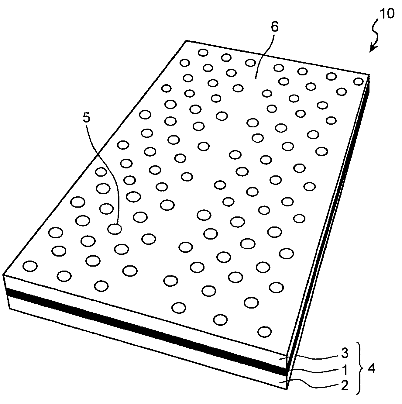
[0044]FIG. 1 is a perspective view that shows the configuration of the optical active device according to the present invention. The optical active device10 according to this invention is constructed by forming triangular lattice-form periodic air hole structures 5 in a two-dimensional plane of a slab layer 4 formed by sequentially laminating a lower cladding layer 2 comprising InGaAsP, an active layer 1 having a multiple quantum well (hereinafter “MQW”) structure comprising InGaAsP, and an upper cladding layer 3 comprising InGaAsP on a substrate (not shown) comprising InP or the like, so as to go through the slab layer 4 in a direction of lamination. A defect (a linear defect with respect to the two-dimensional periodic structure) 6 in which the periodic air hole structures 5 in this two-dimensional plane are linearly broken is further formed. By the periodic air hole structure 5 in the two-dimensional plane formed in the slab layer 4, a periodic refractive index distribution struc...

second embodiment

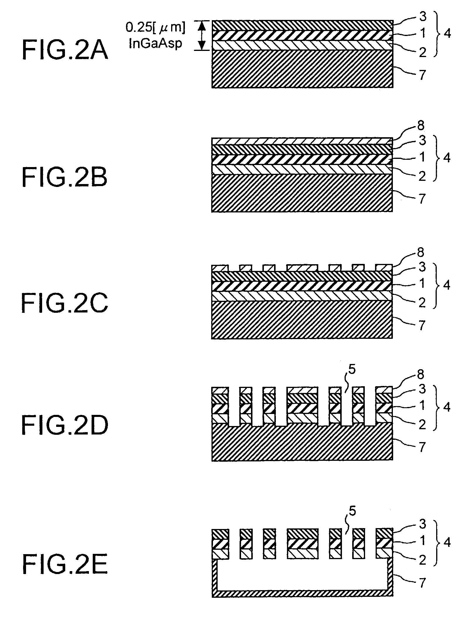
[0063]FIG. 6 is a perspective view that shows the configuration of the optical active device according to the present invention. As shown in FIG. 6, the optical active device is constructed such that the active layer 1 exists only in the linear defect region 6 formed in a two-dimensional plane of a cladding layer 20, and the active layer 1 does not exist in the region of the air hole structures 5 for forming the refractive index periodic structure.

[0064]FIGS. 7A to 7E are sectional views that schematically show a production method of the optical active device composed of the two-dimensional slab photonic crystal structure shown in FIG. 6. Here, an example in which InP is used for the substrate, and InGaAsP is used for the active layer 1 and the cladding layer 20 is explained. As shown in FIG. 7A, the lower cladding layer 2 consisting of InGaAsP, and the active layer 1 consisting of InGaAsP, in which the film thickness of the quantum well layer and the barrier layer, the number of la...

third embodiment

[0074]In the third embodiment, laser oscillation from the edge of the linear defect region 6 or from the point (isolated) defect 31 or 32 becomes possible, by adequately designing the position of the linear defect region 6 and the point (isolated) defect 31 or 32. FIG. 10 is a perspective view that shows the structure of an optical active device, when laser oscillation is generated from a point (isolated) defect. As shown in FIG. 10, when the both ends of the linear defect region 6 are terminated by the two-dimensional refractive index periodic structure, more specifically, when air hole structures 5a and 5b are provided at the both ends of the linear defect region 6, so as to match with the period of the ambient air hole structures 5, the light cannot propagate to the ends of the linear defect region 6, and the amplified laser beams are emitted only from the point (isolated) defect 31 where the compound resonator is formed. By such a configuration, a high-output laser device with l...


PUM

PropertyMeasurementUnit
refractive indexaaaaaaaaaa

Abstract

In an optical device, a slab layer has an active layer sandwiched between two cladding layers. Periodic air holes are present in the slab layer. A linear defect region is present in a part of the air hole structures. As a result, laser oscillation is generated at the band end in a two-dimensional photonic crystal waveguide mode.

Description

BACKGROUND OF THE INVENTION[0001]1) Field of the Invention[0002]The present invention relates to an optical active device using a two-dimensional slab photonic crystal, in which an optical control function is improved, in an optical device used for optical transmission and optical information processing.[0003]2) Description of the Related Art[0004]A photonic crystal is an optical material having a periodic refractive index distribution, and has a band structure, with respect to an optical energy, that is the same as for a solid crystal, including a band structure, with respect to an electronic energy due to a periodic potential distribution. A photonic crystal is obtained by, for example, periodically arranging materials having different refractive indexes multidimensionally. Such a photonic crystal reveals new optical properties such as dispersibility and anisotropy that cannot be obtained by conventional optical materials, and hence has been noted as a next generation element in o...

Claims


Application Information

Patent Timeline
Patent Type & Authority Patents(United States)
IPC IPC(8): G02B6/10G02B6/12G02B6/122G02F1/025H01S5/10H01S5/50
CPCG02B6/1225B82Y20/00
Inventor SUGITATSU, ATSUSHINODA, SUSUMU
Owner MITSUBISHI ELECTRIC CORP
Why Eureka
Try Eureka