Semiconductor device and method for manufacturing the same

a technology of semiconductors and semiconductors, applied in the direction of semiconductor devices, electrical devices, transistors, etc., can solve the problems of reducing the manufacturing yield, increasing the manufacturing process, and raising the manufacturing cost, so as to reduce the yield and reduce the manufacturing cost. , the effect of high withstanding voltag

Inactive Publication Date: 2007-03-13
SEMICON ENERGY LAB CO LTD
View PDF25 Cites 7 Cited by
  • Summary
  • Abstract
  • Description
  • Claims
  • Application Information

AI Technical Summary

Benefits of technology

[0036]Since the configurations of the present invention makes it possible to control the carrier density between the source region or drain region and the channel forming region without forming the LDD region, misalignment of a mask used in a process for forming the LDD region can be avoided, and thus decrease in yield can be restrained.
[0037]According to the configurations of the present invention, a number of TFTs having gate insulating films each having different thickness can be formed on a same substrate without using a special process. Moreover, even if the LDD region is not formed, an optional voltage is applied to the first auxiliary electrode and second auxiliary electrode, thereby the carrier density in the semiconductor layer under respective auxiliary electrodes can be changed.
[0038]In addition, a TFT having a thick gate insulating film is used as a TFT for a driving circuit such as a shift register circuit, level shifter circuit, buffer circuit, or sampling circuit and a pixel TFT, thereby a TFT, which has a high withstanding voltage, enables a low power consumption design, and has a high reliability, can be made. Furthermore, a TFT having a short channel length and a thin gate insulating film is used as a TFT for functional circuits including CPU, DRAM, an image processing circuit, and an audio processing circuit, thereby operating characteristics and reliability can be improved.

Problems solved by technology

In addition, there is a problem of increase in the manufacturing process for its complexity in forming a TFT having an LDD structure and a TFT wherein an LDD region is overlapped with a gate electrode with a gate insulating film interposed therebetween.
It is obvious that the increase in the manufacturing process raises the manufacturing cost and also lowers the manufacturing yield.
And misalignment may cause the problem of reduction in yield.

Method used


Image

  • Semiconductor device and method for manufacturing the same
  • Semiconductor device and method for manufacturing the same
  • Semiconductor device and method for manufacturing the same

Examples


embodiment mode 1

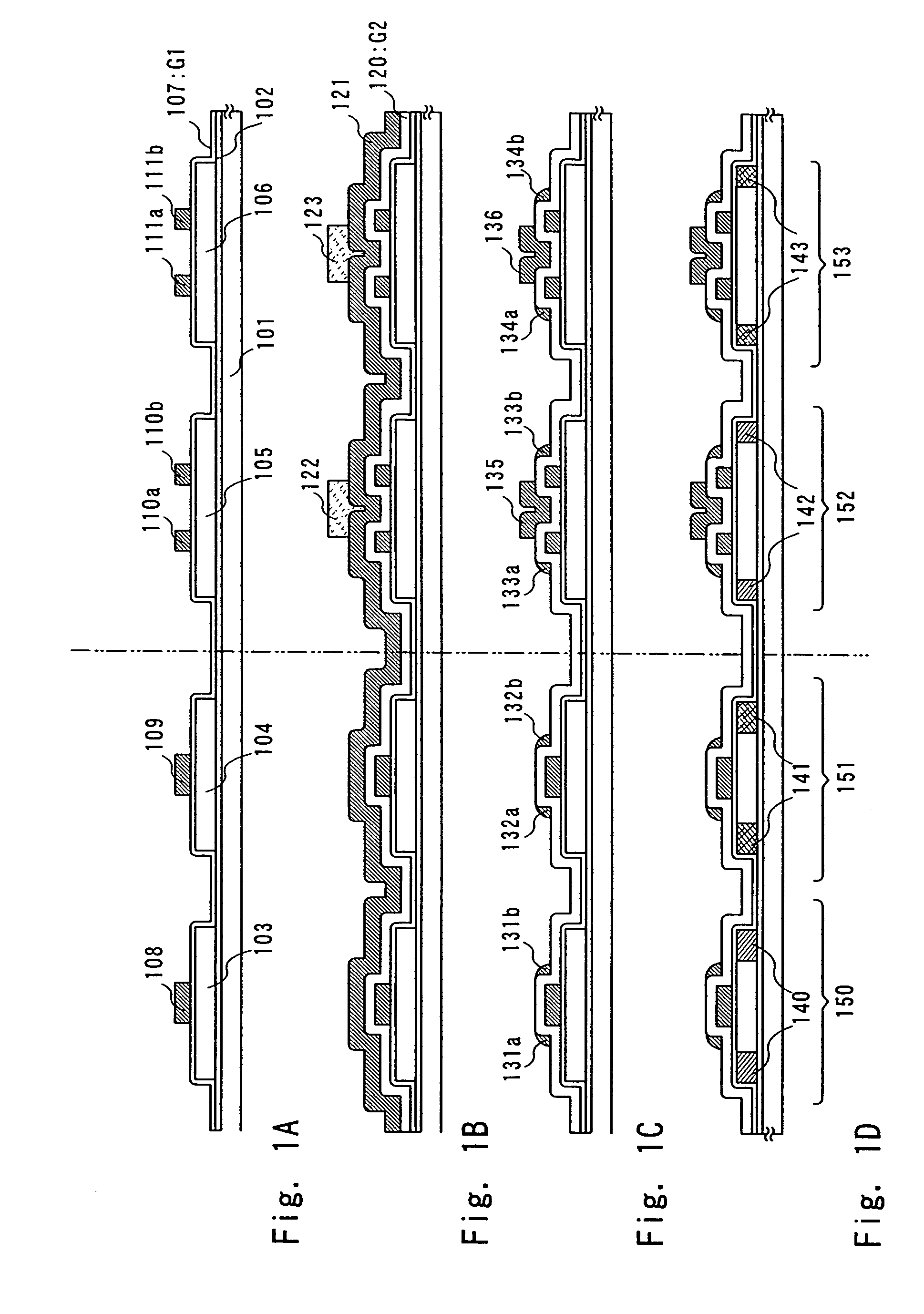
[0053]An example of the invention is shown in FIGS. 1A–1D. This embodiment shows a process where a P-TFT and N-TFT having a thin gate insulating film and first auxiliary electrodes (in FIGS. 1A–1D, TFT comprising the gate insulating film G1), and a P-TFT and N-TFT having a thick gate insulating film, first auxiliary electrodes, and second auxiliary electrodes (in FIGS. 1A–1D, TFT comprising the gate insulating film G1 and G2) are formed at the same time.

[0054]As shown in FIG. 1A, a crystalline semiconductor film is formed on a substrate 101 through an insulating film 102 as a base film, then the crystalline semiconductor film is etched in an optional pattern and thus separated crystalline semiconductor films 103 to 106 are formed. Then, a first gate insulating film (hereinafter, shown as G1 in the embodiment and FIGS. 1A–1D) 107 is deposited. Typically, the first gate insulating film (G1) 107 functions as a gate insulating film for a TFT for a driving circuit to which a fast operati...

embodiment mode 2

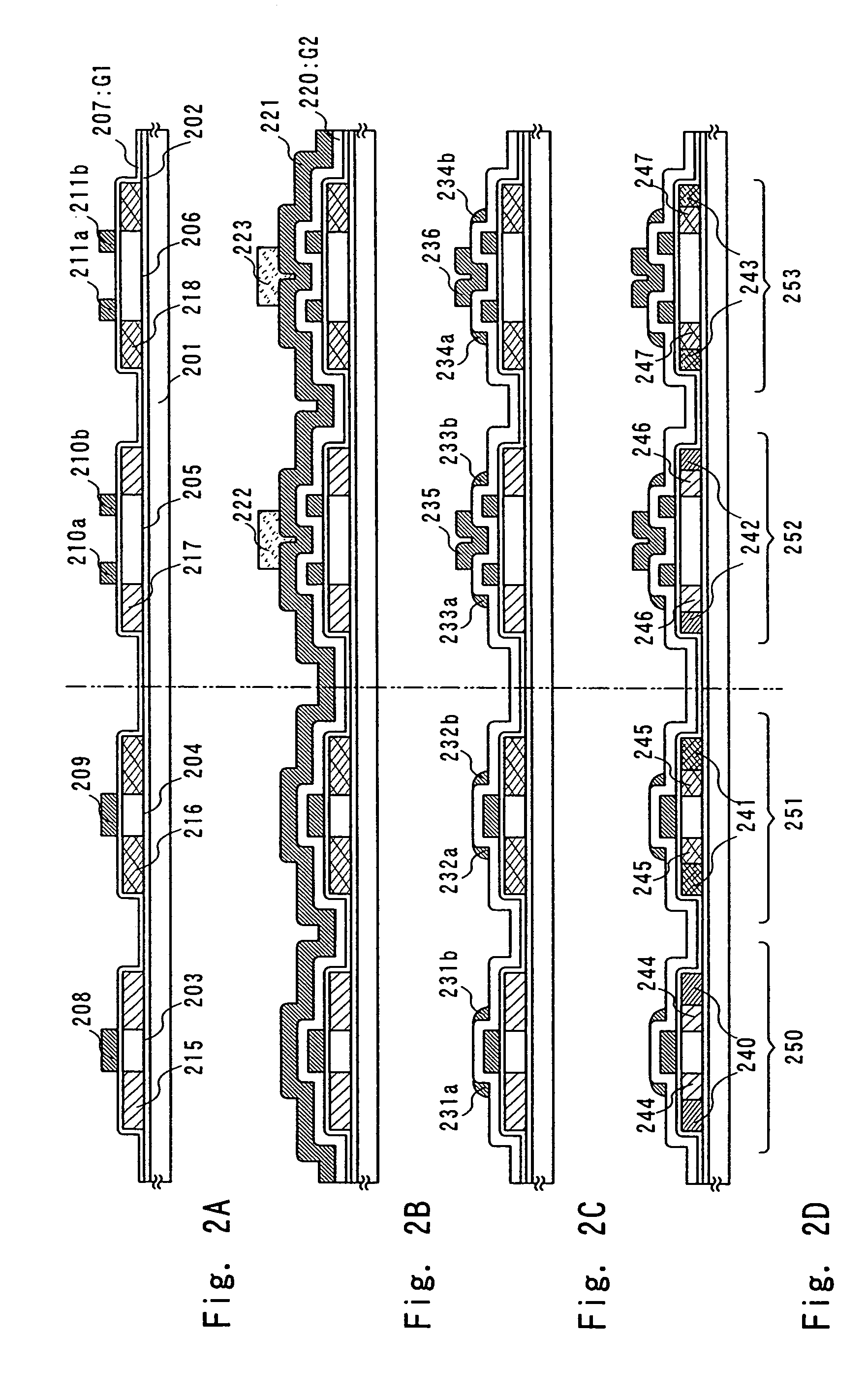
[0067]An example of the invention is shown in FIGS. 2A–2D. The embodiment shows a process for forming a TFT having the LDD region in the active matrix substrate described in the first embodiment.

[0068]As shown in FIG. 2A, a crystalline semiconductor film is formed on a substrate 201 through an insulating film 202 as a base film, and then the crystalline semiconductor film is etched in an optional pattern and thus separated crystalline semiconductor films 203 to 206 are formed. Then, a first gate insulating film (hereinafter, shown as G1 in the embodiment and FIGS. 2A–2D) 207 is deposited. The first gate insulating film (G1) 207 has a small thickness, and the thickness of the first gate insulating film is 1 to 100 nm, preferably 5 to 50 nm.

[0069]Next, a first conductive film is deposited, then masks (not shown) are formed using the photolithography technique, then an unnecessary area in the first conductive film is removed using a known etching method, and thus first gate electrodes ...

embodiment mode 3

[0080]An example of the invention is shown in FIGS. 3A–3D. In this embodiment, the second auxiliary electrodes are formed only in the TFT having the thin gate insulating film (in FIGS. 3A–3D, TFT in which the gate insulating film comprises G1) in the active matrix substrate described in the first embodiment.

[0081]As shown in FIG. 3A, a crystalline semiconductor film is formed on a substrate 301 through an insulating film 302 as a base film, and then the crystalline semiconductor film is etched in an optional pattern and thus separated crystalline semiconductor films 303 to 306 are formed. Then, a first gate insulating film (hereinafter, shown as G1 in the embodiment and FIGS. 3A–3D) 307 is deposited. The first gate insulating film (G1) 307 has a small thickness, and the thickness of the first gate insulating film is 1 to 100 nm, preferably 5 to 50 nm.

[0082]Next, a first conductive film is deposited, then masks (not shown) are formed using the photolithography technique, then an unne...


PUM


Abstract

It is an object of the present invention to form a TFT which is required to have a high withstanding voltage characteristic as well as to lower an off-current, a TFT which is required to have a high withstanding voltage characteristic as well as to raise an on-current, and a TFT in which a short channel structure and the decline in the threshold voltage arising therefrom are attached importance to, on one and the same substrate. A TFT having gate insulating films with different thickness can be formed on one and the same substrate by providing auxiliary electrodes in addition to the gate electrodes over a semiconductor film as well as laminating the insulating films.

Description

BACKGROUND OF THE INVENTION[0001]1. Field of the Invention[0002]The present invention relates to a semiconductor device which comprises a circuit formed from a thin film transistor (hereinafter referred to as TFT) and the manufacturing method thereof. The present invention further relates to a display module typified by an active matrix liquid crystal module and an EL module, each fabricated using a TFT, and also to an electronic device which comprises such display modules as its components.[0003]2. Description of the Related Art[0004]Recently, the development of a semiconductor device having a large-scale integrated circuit formed from a TFT has been advanced. The TFT comprises a thin semiconductor film (with a thickness of about several to several hundred nanometers) formed over a substrate having an insulating surface. An active matrix liquid crystal display device, an EL display device, and a close coupling image sensor are known as typical examples of the semiconductor devices....

Claims


Application Information

Patent Timeline
Patent Type & Authority Patents(United States)
IPC IPC(8): H01L29/04H01L31/036H01L31/0376H01L31/20H01L21/336H01L21/77H01L21/84H01L27/12H01L29/49H01L29/786
CPCH01L27/12H01L29/4908H01L27/124H01L29/78645H01L29/78675H01L29/66757
Inventor ARAO, TATSUYA
Owner SEMICON ENERGY LAB CO LTD
Why Eureka
Try Eureka