Light-emitting device with coating film on portions of substrates and sealing member

a technology of coating film and substrate, applied in the direction of non-linear optics, identification means, instruments, etc., can solve the problems of minute dlc film and hardness, and achieve the effects of high efficiency, easy to scratch or the like, and altering the quality and color of organic resin substrates

Inactive Publication Date: 2007-03-13
SEMICON ENERGY LAB CO LTD
View PDF48 Cites 47 Cited by
  • Summary
  • Abstract
  • Description
  • Claims
  • Application Information

AI Technical Summary

Benefits of technology

[0018]As is apparent from this, if a display device produced with a light-emitting element including an organic resin substrate is left standing in the air for a long time period, moisture gradually permeates and the organic light-emitting element is degraded. In addition, a sealing member used to seal a light-emitting element is also made of an organic resin material, so that it is difficult to completely prevent oxygen and moisture in the air from entering through sealed portions.
[0019]Also, an organic resin substrate is soft, in comparison with a metal substrate or a glass substrate, so that scratches or the like are easily made thereon. Further, the long-term exposure to the direct sunlight causes a light chemical reaction and alters the quality and color of the organic resin substrate.
[0020]As described above, the organic resin substrate is a highly effective means to realize a display device reduced in weight with high shock resistance, although there remain many problems that must be solved in order to ensure the reliability of the light-emitting element. In view of these problems, the object of the present invention is to provide a display device that uses a light-emitting element with a high degree of reliability.
[0021]Also, if the outside light (the light existing outside the light-emitting device) enters picture elements that do not emit light, the light is reflected by the back surface (the surface contacting the organic compound layer) of the cathode,

Problems solved by technology

In the latter case, the DLC

Method used


Image

  • Light-emitting device with coating film on portions of substrates and sealing member
  • Light-emitting device with coating film on portions of substrates and sealing member
  • Light-emitting device with coating film on portions of substrates and sealing member

Examples


embodiment mode 1

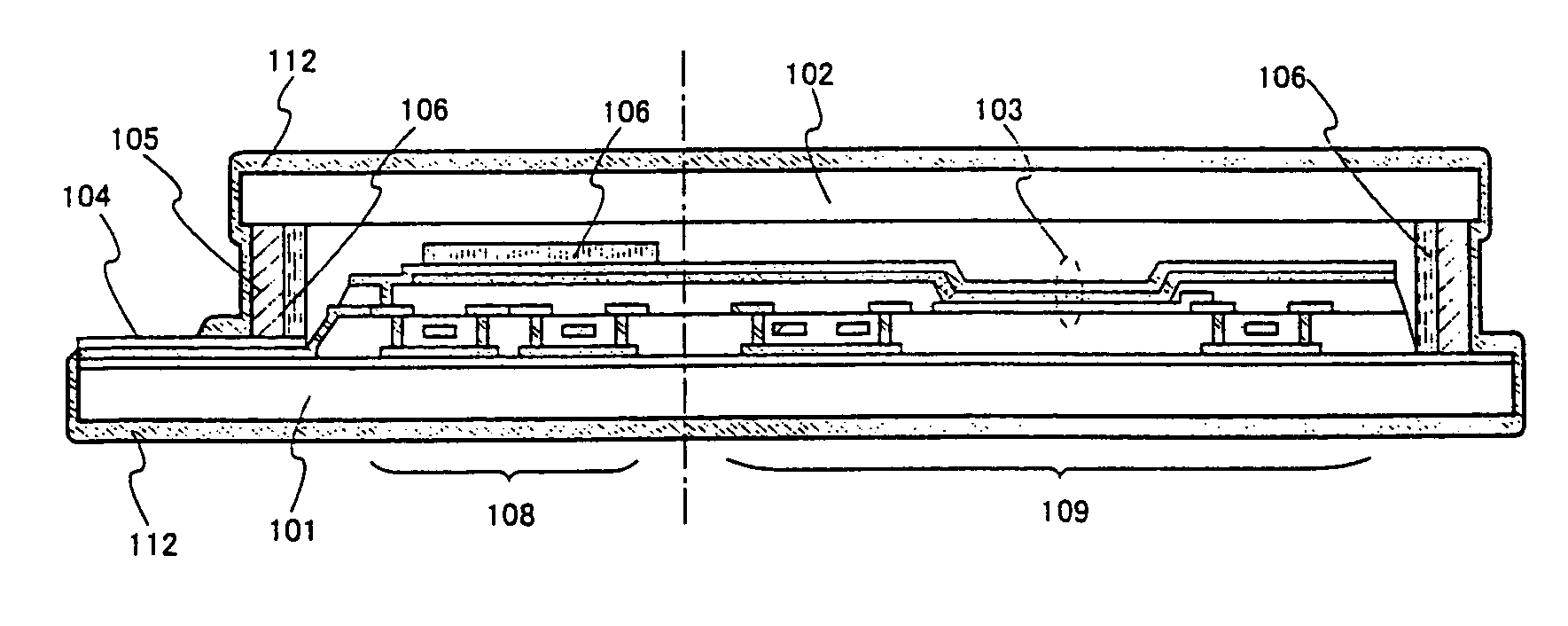
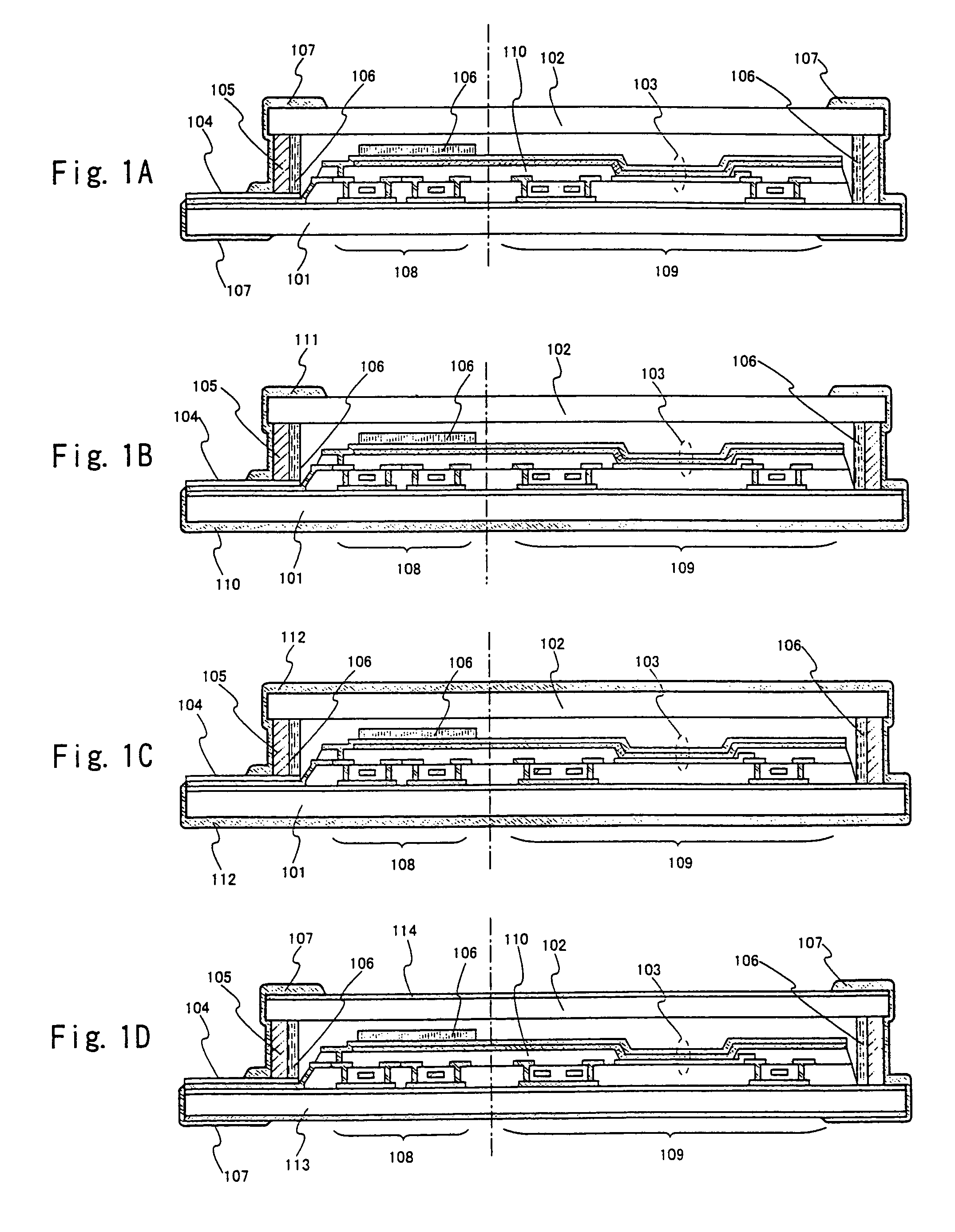
[0054]Embodiment Mode 1 is described below with reference to FIGS. 1A to 1D each showing a display device using a light-emitting element. FIG. 1A shows a state where an element substrate 101, on which a driving circuit 108 and a pixel portion 109 are formed using TFTs (thin-film transistors) and a sealing substrate 102 are fixed using a sealing member 105. A light-emitting element 103 is formed in the sealed space formed between the element substrate 101 and the sealing substrate 102. A dryer agent 106 is provided on the driving circuit or in the vicinity of the sealing member 105. It should be noted here that although not shown in this drawing, the dryer agent 106 may be contained in a partition wall 110 that is formed across the pixel portion 109 and the driving circuit 108.

[0055]Each of the element substrate and sealing substrate is made of an organic resin material, such as polyimide, polyethylene terephthalate (PET), polyethylene naphthalate (PEN), polyether sulfone (PES), or a...

embodiment mode 2

[0067]FIGS. 14A and 14B each show an example where a pixel portion and a driving circuit are formed on a substrate having an insulating surface (such as a glass substrate, a ceramic substrate, a crystallized glass substrate, a metal substrate, or a plastic substrate).

[0068]In these drawings, reference numeral 1401 represents a gate-side driving circuit; numeral 1402, a source-side (data-side) driving circuit; and numeral 1403, a pixel portion. Signals transmitted to the gate-side driving circuit 1401 and the source-side driving circuit 1402 are supplied from an FPC (flexible print circuit) 1405 via input wiring 1404.

[0069]A sealing substrate 1406 is used to seal light-emitting elements. The light-emitting elements emit light toward the sealing substrate 1406, so that the sealing substrate 1406 is required to have transparency. Numeral 1407 represents a sealing resin used to seal the sealing substrate 1406 and the element substrate 1400. A cross-sectional view taken along the line A–...

embodiment 1

[0081]The present invention is applicable to various types of display devices so long as the display devices use light-emitting elements. FIG. 4 shows an example of display device to which the present invention is applied. The display device in this drawing is an active matrix type display device produced using TFTs. TFTs are classified into amorphous silicon TFTs and polysilicon TFTs, depending on what materials are used to produce semiconductor films that form channel formation regions. The present invention is applicable to both types of TFTs.

[0082]It is impossible to produce an organic resin substrate, which is resistant to heat processing at 450° C. or higher, using a commercially available material. A laser anneal technique, however, makes it possible to produce polysilicon TFTs only by heating the substrate to 300° C. or below. Also, in many cases, hydrogenation processing is required to be performed during the production of polysilicon TFTs. A plasma-aided hydrogenation proc...


PUM


Abstract

Although an organic resin substrate is highly effective at reducing the weight and improving the shock resistance of a display device, it is required to improve the moisture resistance of the organic resin substrate for the sake of maintaining the reliability of an EL element. Hard carbon films are formed to cover a surface of the organic resin substrate and outer surfaces of a sealing member. Typically, DLC (Diamond like Carbon) films are used as the carbon films. The DLC films have a construction where carbon atoms are bonded into an SP3 bond in terms of a short-distance order, although the films have an amorphous construction from a macroscopic viewpoint. The DLC films contain 95 to 70 atomic % carbon and 5 to 30 atomic % hydrogen, so that the DLC films are very hard and minute and have a superior gas barrier property and insulation performance.

Description

BACKGROUND OF THE INVENTION[0001]1. Field of the Invention[0002]The present invention relates to a device (hereinafter referred to as a light-emitting device) that has an element (hereinafter referred to as a light-emitting element) where a thin film including a luminescent material is sandwiched between a pair of an anode electrode and a cathode electrode. In particular, the present invention relates to a light-emitting device whose light-emitting element includes a thin film (hereinafter referred to as a light-emitting layer) made of an electro-luminescent material (EL material). The present invention also relates to a display device that uses a substrate made of an organic resin material and, more particularly, to a display device where a pixel portion is formed on such a substrate using thin-film transistors and an EL material.[0003]2. Description of the Related Art[0004]Liquid crystal panels or EL materials applied to display devices may contribute to reduction in weight and th...

Claims


Application Information

Patent Timeline
IPC IPC(8): H01L29/04H05B33/04G09F9/30H01L27/32H01L51/50H01L51/52H01L51/56H05B33/14
CPCH01L27/32H01L51/5221H01L51/5246H01L51/5253H01L51/5281H01L27/3246H01L51/5237H01L27/12H01L27/1214H01L27/3244H01L29/78603H01L51/56H01L2251/5338H10K59/00H10K59/12H10K50/82H10K50/846H10K50/841H10K50/8426H10K50/86H10K50/844H10K2102/311H10K71/00H10K59/1213H10K50/84H10K59/122H10K59/1201
Inventor YAMAZAKI, SHUNPEIARAI, YASUYUKI
Owner SEMICON ENERGY LAB CO LTD
Why Eureka
Try Eureka