Method for fabricating an interference display unit

a technology of interference display and manufacturing method, which is applied in the direction of photomechanical equipment, instruments, originals for photomechanical treatment, etc., can solve the problems of high cost of complicated manufacturing process and yield increase, and achieve the effect of high brightness

Inactive Publication Date: 2007-04-03
SNAPTRACK
View PDF388 Cites 144 Cited by
  • Summary
  • Abstract
  • Description
  • Claims
  • Application Information

AI Technical Summary

Benefits of technology

[0018]It is therefore an objective of the present invention to provide a method for manufacturing an optical interference display un

Problems solved by technology

The cost of the complicated manufacturing process is higher, and the y

Method used


Image

  • Method for fabricating an interference display unit
  • Method for fabricating an interference display unit
  • Method for fabricating an interference display unit

Examples


embodiment 1

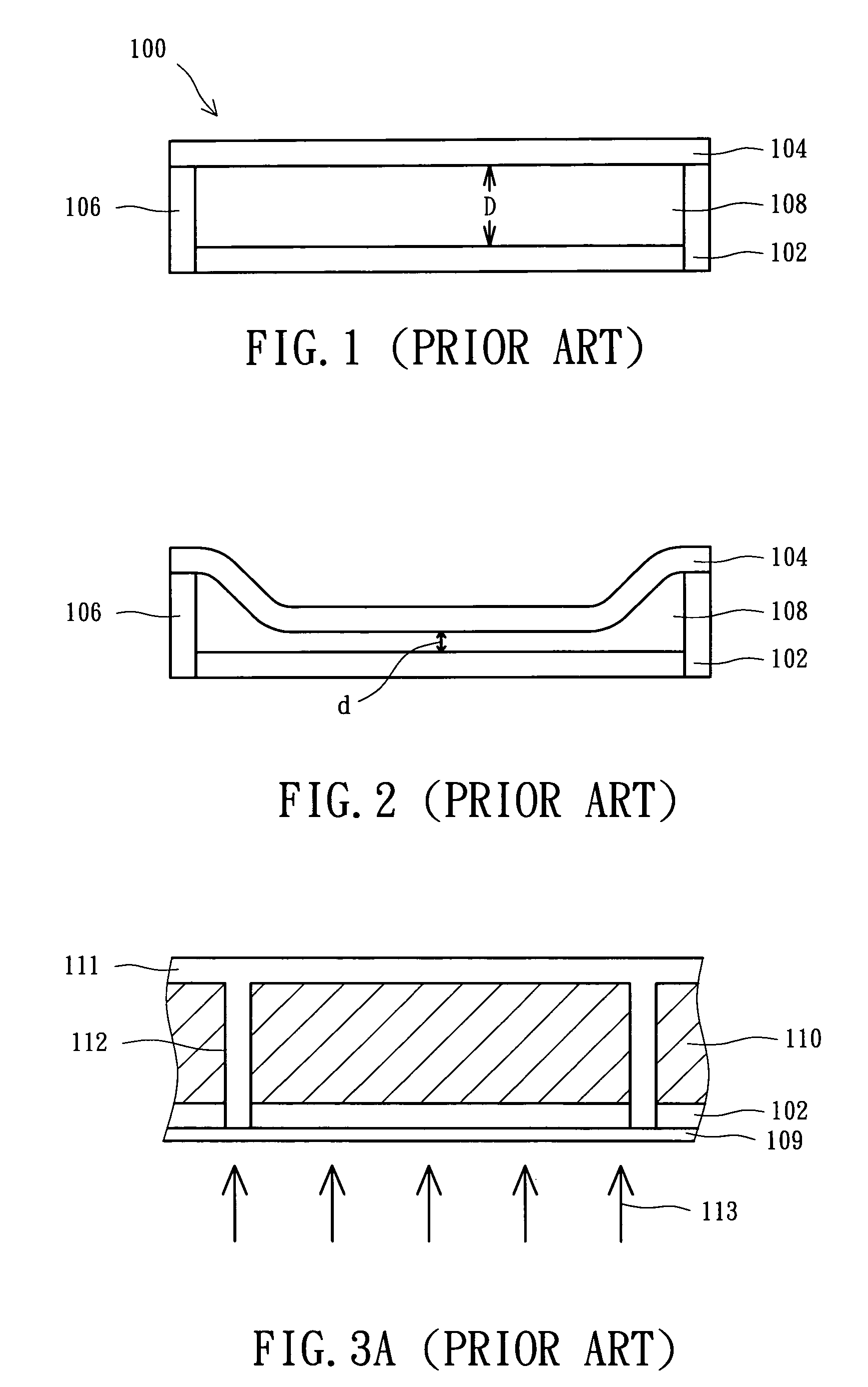
[0039]FIGS. 6A to 6C depict a method for manufacturing an optical interference display unit according to a preferred embodiment of the invention. Please referring to FIG. 6A first, a first electrode 502 and a sacrificial layer 506 are formed in order on a transparent substrate 501. The sacrificial layer 506 is made of transparent materials such as dielectric materials, or opaque materials such as metal materials. An opening 508 is formed in the first electrode 502 and the sacrificial layer 506 by a photolithographic etch process. The opening 508 is suitable for forming a post therein.

[0040]Next, a material layer 510 is formed in the sacrificial layer 506 and fills the opening 508. The material layer 510 is suitable for forming posts, and the material layer 510 generally uses photosensitive materials such as photoresists, or non-photosensitive polymer materials such as polyester, polyamide or the like. If non-photosensitive materials are used for forming the material layer 510, a pho...

embodiment 2

[0046]FIGS. 7A to 7D depict a method for manufacturing a matrix color planar display structure according to the second preferred embodiment of this invention. Reference is made to FIG. 7A first, illustrating formation of the first electrode 602 and a sacrificial layer 604 in order on a transparent substrate 601. The sacrificial layer 604 can be made of transparent materials such as dielectric materials, or opaque materials such as metal materials. Openings 606, 608, 610, and 612 are formed in the first electrode 602 and the sacrificial layer 604 by a photolithographic etch process, and openings 606, 608, 610, and 612 are suitable for forming posts therein.

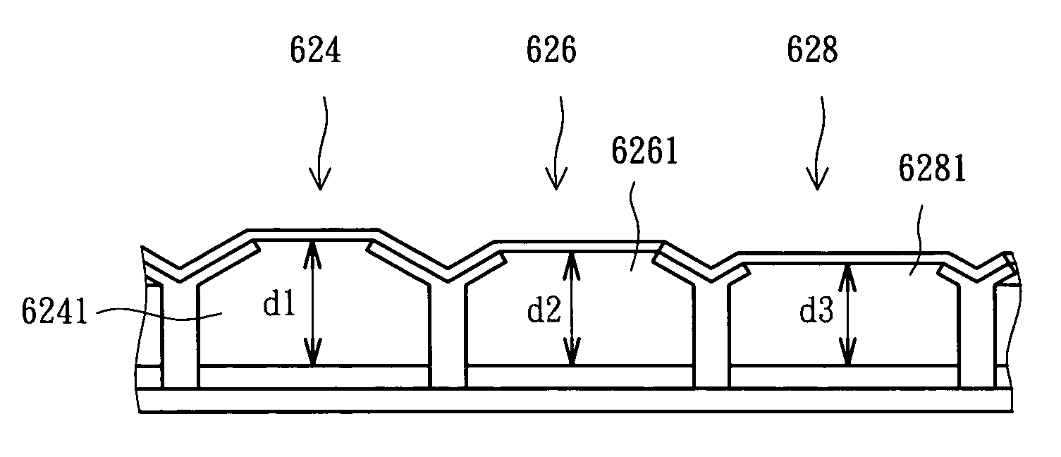
[0047]Next, a material layer 614 is formed on the sacrificial layer 604 and fills the openings 606, 608, 610, and 612. The optical interference display unit 624 is defined by openings 606 and 608, the optical interference display unit 626 is defined by openings 608 and 610, and the optical interference display unit 628 is defined b...


PUM


Abstract

A method for fabricating an interference display unit is provided. A first plate and a sacrificial layer are formed in order on a substrate and at least two openings are formed in the first plate and the sacrificial layer. A photoresist layer is spin-coated on the sacrificial layer and fills the openings. A photolithographic process patterns the photoresist layer to define a support with an arm. A second plate is formed on the sacrificial layer and posts. The arm's stress is released through a thermal process. The position of the arm is shifted and the distance between the first plate and the second plate is therefore defined. Finally, The sacrificial layer is removed.

Description

FIELD OF INVENTION[0001]The present invention relates to a method for manufacturing an optical interference display. More particularly, the present invention relates to a method for manufacturing an optical interference display with posts of arms.BACKGROUND OF THE INVENTION[0002]Planar displays are popular for portable displays and displays with space limits because they are light and small in size. To date, planar displays in addition to liquid crystal displays (LCD), organic electro-luminescent displays (OLED), plasma display panels (PDP) and so on, as well as a mode of the optical interference display are of interest.[0003]U.S. Pat. No. 5,835,255 discloses an array of display units of visible light that can be used in a planar display. Please refer to FIG. 1, which depicts a cross-sectional view of a display unit in the prior art. Every optical interference display unit 100 comprises two walls, 102 and 104. Posts 106 support these two walls 102 and 104, and a cavity 108 is subseq...

Claims


Application Information

Patent Timeline
IPC IPC(8): H01L21/00G02B26/00G02F1/21G03C5/00G03F7/00
CPCG02B26/001B81C1/00182B81B2201/047G03F7/0007G02B26/00
Inventor LIN, WEN-JIANTSAI, HSIUNG-KUANG
Owner SNAPTRACK
Why Eureka
Try Eureka