Method of manufacturing piezoelectric device

a piezoelectric device and piezoelectric technology, applied in the direction of device material selection, conductive pattern formation, generator/motor, etc., can solve the problems of poor orientation, difficult piezoelectric layer or ferroelectric layer formation, and difficulty in forming a piezoelectric layer or ferroelectric layer, etc., to achieve easy manufacturing, low cost, and easy manufacturing

Active Publication Date: 2007-04-10
SEIKO EPSON CORP
View PDF7 Cites 10 Cited by
  • Summary
  • Abstract
  • Description
  • Claims
  • Application Information

AI Technical Summary

Benefits of technology

[0008]Exemplary embodiments of the present invention address the above discussed and / or other problems, and provides a method of manufacturing a piezoelectric device including a piezoelectric layer that has high crystallinity in which crystal orientation is aligned to a desired orientation. Exemplary embodiments further provide a method of manufacturing a ferroelectric device including a ferroelectric layer that has similar high crystallinity, a droplet ejection head, and electronic equipment that incorporate a piezoelectric device or ferroelectric device and thus have high reliability.
[0059]The electronic equipment of exemplary embodiments of the present invention includes a piezoelectric device manufactured by any of the above exemplary methods of manufacturing a piezoelectric device, or a ferroelectric device manufactured by any of the above exemplary methods of manufacturing a ferroelectric device. According to exemplary embodiments of this invention, the electronic equipment having a piezoelectric device or a ferroelectric device that is easily manufactured at low cost and is superior in characteristics, can be provided.

Problems solved by technology

However, in the related art, forming a lower electrode having a desired orientation is difficult.
Accordingly, there is a problem in that it is difficult to form a piezoelectric layer or ferroelectric layer whose crystal orientation is aligned to a desired direction, on the lower electrode with poor orientation.

Method used


Image

  • Method of manufacturing piezoelectric device
  • Method of manufacturing piezoelectric device
  • Method of manufacturing piezoelectric device

Examples


first exemplary embodiment

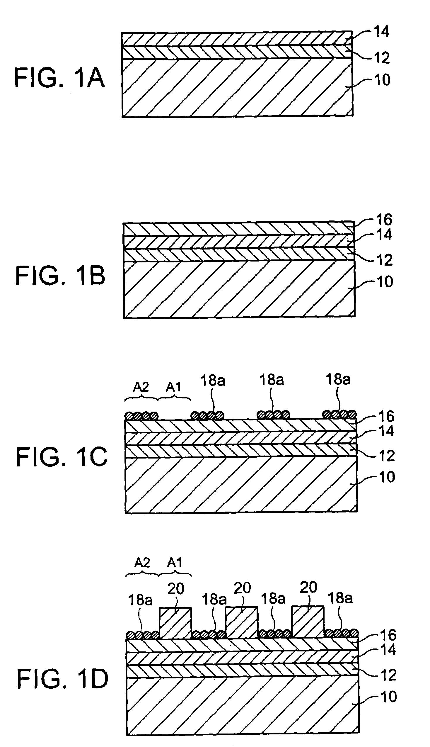
[0077]FIGS. 1A–1D are schematics showing a method of manufacturing a piezoelectric device according to a first exemplary embodiment of the present invention

[0078]In the present exemplary embodiment, first, as shown in FIG. 1A, a process of forming an insulating layer 12 and a buffer layer 14 on a substrate 10 is implemented. The substrate 10 is a (110)-oriented silicon single crystal wafer of diameter of 100 millimeters and thickness of 200 micrometers, for example. The insulating layer 12 is formed by disposing the substrate 10 in a furnace whose temperature is set to about 1100 degrees centigrade and flowing dry oxygen so as to carry out thermal oxidation for about 22 hours. The insulating layer 12 is composed of silicon dioxide (SiO2) and is formed by about 1 micrometers of film thickness.

[0079]The insulating layer 12 may be formed by using a film forming method such as CVD (Chemical Vapor Deposition) besides the thermal oxidation. The insulating layer 12 may be formed of, beside...

second exemplary embodiment

(Second Exemplary Embodiment)

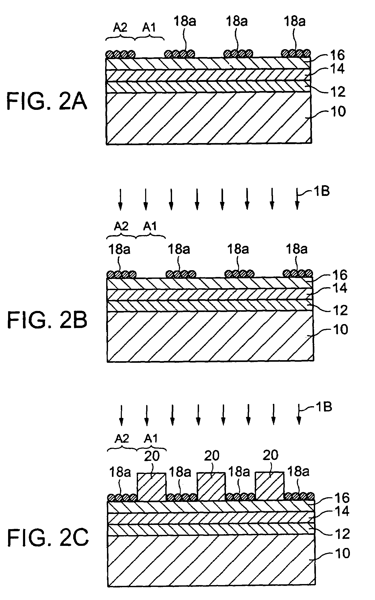
[0100]FIGS. 2A–C are schematics showing a method of manufacturing a piezoelectric device according to a second exemplary embodiment of the present invention.

[0101]As shown in FIG. 2A, also in the present exemplary embodiment, in the same way as that of the first exemplary embodiment, the insulating layer 12, the buffer layer 14, and the lower electrode 16 are formed on the substrate 10 in sequence, and then the self-assembled monolayers 18a are formed on given regions on the lower electrode 16. Thereby, the high affinity regions (first regions) A1 and the low affinity regions (second regions) A2 are formed.

[0102]Next, at the same time that a solution of a material including the substance of the piezoelectric layers 20 is supplied onto the lower electrode 16 as a mist, an ion beam IB is radiated to the lower electrode 16 as shown in FIG. 2B, so as to start the forming of the piezoelectric layers 20 by an ion beam assisted method. In the present exemplary ...

third exemplary embodiment

(Third Exemplary Embodiment)

[0104]FIGS. 3A–C are schematics showing a method of manufacturing a piezoelectric device according to a third exemplary embodiment of the present invention.

[0105]As shown in FIG. 3A, also in the present exemplary embodiment, in the same way as that of the first exemplary embodiment, the insulating layer 12, the buffer layer 14, and the lower electrode 16 are formed on the substrate 10 in sequence, and then the self-assembled monolayers 18a are formed on given regions on the lower electrode 16. Thereby, the high affinity regions (first regions) A1 and the low affinity regions (second regions) A2 are formed.

[0106]Next, as with the second exemplary embodiment, at the same time that a solution of a material including the substance of the piezoelectric layers is supplied onto the lower electrode 16 as a mist, the ion beam IB is radiated to the lower electrode 16, so as to start the forming of the piezoelectric layers by an ion beam assisted method. In the pres...


PUM

PropertyMeasurementUnit
radiation angleaaaaaaaaaa
wavelengthaaaaaaaaaa
thicknessaaaaaaaaaa

Abstract

Exemplary embodiments of the present invention provide a method of manufacturing a piezoelectric device that includes a piezoelectric layer having high crystallinity in which crystal orientation is aligned to a desired direction, a method of manufacturing a ferroelectric device that includes a ferroelectric layer having the similar high crystallinity, and so forth. Exemplary embodiments include an insulating layer composed of SiO2 and so forth and a buffer layer composed of strontium oxide (SrO) and so forth are formed on a substrate such as a silicon single crystal wafer in sequence, and then a lower electrode composed of strontium ruthenate (SRO) is formed on the buffer layer. By forming self-assembled monolayers on the lower electrode, high affinity regions A1 and low affinity regions A2 are formed. Then, piezoelectric layers are selectively formed only on the high affinity regions A1.

Description

BACKGROUND OF THE INVENTION[0001]1. Field of Invention[0002]Exemplary embodiments of the present invention relate to a method of manufacturing a piezoelectric device and a ferroelectric device, a droplet ejection head, and electronic equipment.[0003]2. Description of Related Art[0004]A piezoelectric element, which is a type of a piezoelectric device, has a structure in which a piezoelectric layer composed of a poly-crystal, an upper electrode, and a lower electrode that are disposed in a manner of sandwiching the piezoelectric layer, are included; The piezoelectric element utilizes stress caused in the piezoelectric layer when voltage is applied between the upper and lower electrodes. In addition, a ferroelectric memory (FeRAM), which is a type of ferroelectric device, has a structure in which a ferroelectric layer, an upper electrode, and an lower electrode that are disposed in a manner of sandwiching the ferroelectric layer, are included. A ferroelectric memory is a non-volatile m...

Claims


Application Information

Patent Timeline
Patent Type & Authority Patents(United States)
IPC IPC(8): H04R17/00B41J2/045H01L41/00H01L41/22B41J2/14B41J2/16H01L21/314H01L21/316H01L21/8246H01L27/105H01L41/08H01L41/09H01L41/18H01L41/187H01L41/317H01L41/319H01L41/331H01L41/39H04R31/00H05K3/20
CPCB41J2/1609B41J2/161B41J2/1612B41J2/1642B82Y30/00H01L21/31691H01L41/318H01L41/319H04R31/00Y10T29/42H04R17/00Y10T29/49128Y10T29/49155H01L41/29H01L21/02197H10N30/06H10N30/078H10N30/079H10N30/80
Inventor TAKAKUWA, ATSUSHIHIGUCHI, TAKAMITSUIWASHITA, SETSUYA
Owner SEIKO EPSON CORP
Why Eureka
Try Eureka