Method for measuring silicide proportion, method for measuring annealing temperature, method for fabricating semiconductor device and x-ray photo receiver

Active Publication Date: 2007-04-10
PANNOVA SEMIC
View PDF4 Cites 0 Cited by
  • Summary
  • Abstract
  • Description
  • Claims
  • Application Information

AI Technical Summary

Benefits of technology

[0021]It is therefore an object of the present invention to provide a method for easily measuring the proportions of a plurality of types of silicides having different compositions with high accuracy. It is another object of the pre

Problems solved by technology

That is, the smaller the resistance or the capacitance is, the faster the Large Scale Integration device operates.
However, if titanium is used, suicides are formed with substantially the same procedure though annealing temperature regions for the RTAs are different.
However, when the pattern width is reduced to 0.1 μm or less, there arise a problem of a break due to migration or the like in silicides and a problem of failure in obtaining a desired low resistance.
To cope with these problems, using various metal elements and adding another material have been studied, but have not been put into actual use yet.
In addition, it is extremely difficult to set the conditions for the second RTA if the proportions of the suicides having different compositions after the first RTA are not within an appropriated range.
However, in the case of measuring the sheet resistance, the proportions cannot be measured directly and the specific resistance also changes depending on the crystallinity of suicides and the like, so that it is extremely diff

Method used


Image

  • Method for measuring silicide proportion, method for measuring annealing temperature, method for fabricating semiconductor device and x-ray photo receiver
  • Method for measuring silicide proportion, method for measuring annealing temperature, method for fabricating semiconductor device and x-ray photo receiver
  • Method for measuring silicide proportion, method for measuring annealing temperature, method for fabricating semiconductor device and x-ray photo receiver

Examples


Example

Embodiment 1

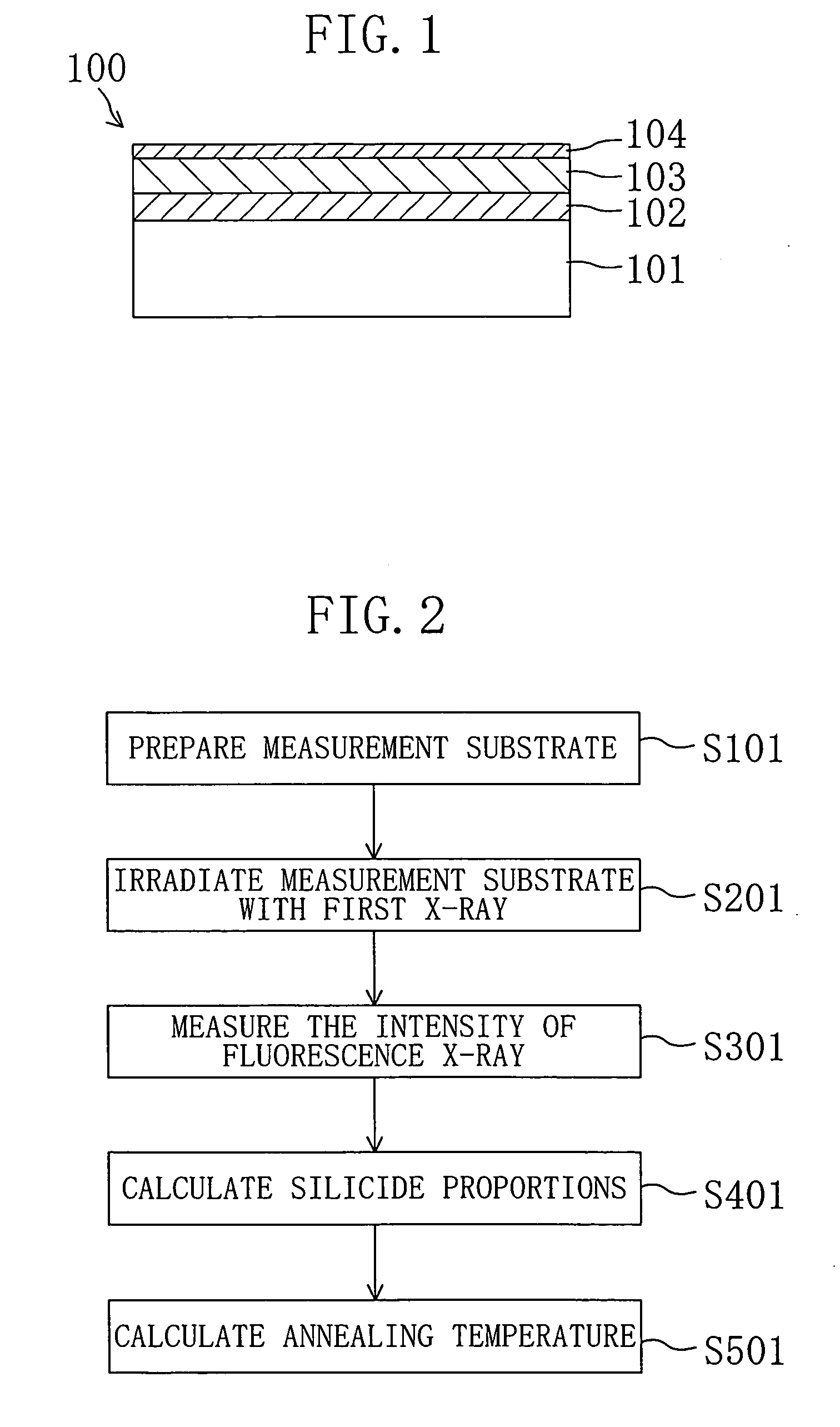
[0049]As shown in FIG. 1, a substrate 100 for measurement (hereinafter, referred to as a measurement substrate) according to this embodiment includes: a silicon substrate (substrate) 101; a silicon oxide film 102; a polysilicon layer 103; and a titanium silicide layer 104. The silicon oxide film 102, the polysilicon layer 103 and the titanium silicide layer 104 are formed on the silicon substrate 101 in this order. A plurality of types of titanium silicides having different compositions included in the titanium silicide layer 104 are formed by a first RTA and have their proportions changed by a second RTA.

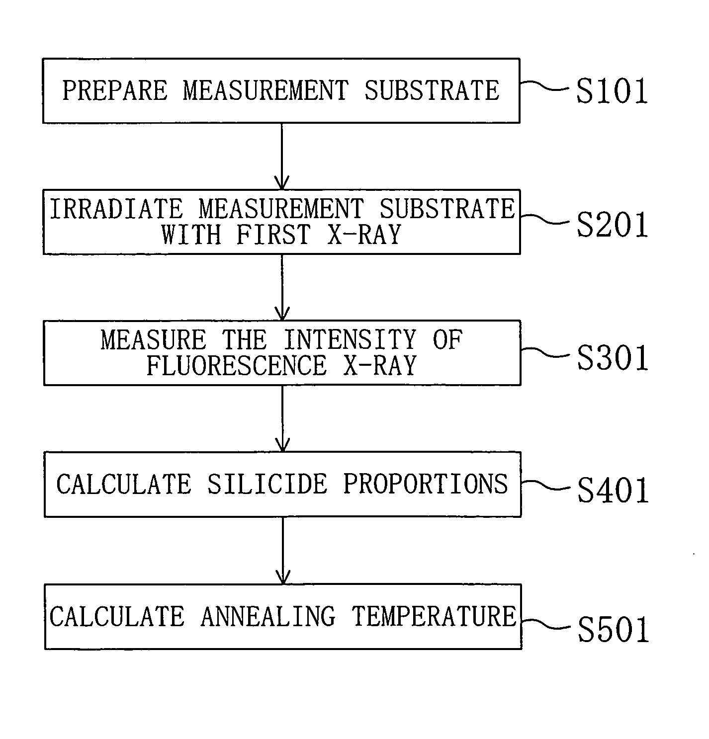
[0050]In this embodiment, an x-ray fluorescence analysis is conducted to measure the proportions of the titanium silicides contained in the titanium silicide layer 104. As shown in FIG. 2, this measurement includes: step S101 of preparing the measurement substrate 100; step S201 of irradiating the measurement substrate 100 with first X-rays; step S301 of measuring the i...

Example

Embodiment 2

[0072]As shown in FIG. 5, a measurement substrate 200 according to this embodiment includes: a silicon substrate (substrate) 201; a doped layer 202 formed by implanting arsenic; and a cobalt silicide layer 203. The doped layer 202 and the cobalt silicide layer 203 are formed over the silicon substrate 201 in this order. A plurality of types of cobalt suicides having different compositions included in the cobalt silicide layer 203 are formed by a first RTA and have their proportions changed by a second RTA.

[0073]In this embodiment, an x-ray fluorescence analysis is performed to measure the proportions of cobalt suicides in the cobalt silicide layer 203. As shown in FIG. 2, this measurement includes: step S101 of preparing the measurement substrate 100; step S201 of irradiating the measurement substrate 100 with first X-rays; step S301 of measuring the intensity of fluorescence X-rays applied; step S401 of calculating the proportions of the suicides from the intensity of t...

Example

Embodiment 3

[0095]As shown in FIG. 8, a measurement substrate 300 according to this embodiment includes: a silicon substrate (substrate) 301; a silicon oxide film 302; a doped layer 303 formed by implanting arsenic; and a cobalt silicide layer 304. The silicon oxide film 302, the doped layer 303 and the cobalt silicide layer 304 are formed over the silicon substrate 301 in this order. A plurality of types of cobalt suicides having different compositions included in the cobalt silicide layer 304 are formed by a first RTA and have their proportions changed by a second RTA.

[0096]In this embodiment, an x-ray fluorescence analysis is conducted to measure the proportions of the cobalt silicides in the cobalt silicide layer 304. As shown in FIG. 2, this measurement includes: step S101 of preparing the measurement substrate 300; step S201 of irradiating the measurement substrate 300 with first X-rays; step S301 of measuring the intensity of fluorescence X-rays applied; and step S401 of calc...


PUM


Abstract

A measurement substrate 100 in which a silicon oxide film 102, a polysilicon layer 103 and a titanium silicide layer 104 are formed over a silicon substrate 101 in this order is prepared. The measurement substrate 100 is irradiated with X-rays so that the proportions of three types of silicides with different compositions in the titanium silicide layer 104 are measured based on the intensity of hard X-rays emitted from oxygen in the silicon oxide film 102 and the intensity of hard X-rays emitted from titanium in the titanium silicide layer 104.

Description

BACKGROUND OF THE INVENTION[0001]The present invention relates to methods for measuring proportions of suicides, methods for measuring annealing temperatures, methods for fabricating semiconductor devices and x-ray photo receivers.[0002]With recent downsizing of semiconductor devices, patterns of LSIs (Large Scale Integration devices) have become finer and finer. Techniques for operating such Large Scale Integration devices with fine patterns at high speed have also been needed. A delay time in an Large Integration devices is mainly determined by the product of a resistance and a capacitance. That is, the smaller the resistance or the capacitance is, the faster the Large Scale Integration device operates. Accordingly, techniques for reducing the resistance of gate electrodes and reducing the resistance of source and drain regions are necessary for increasing the speed of Large Scale Integration devices.[0003]To reduce the resistance, suicides (compounds of silicon with metal, e.g., ...

Claims


Application Information

Patent Timeline
IPC IPC(8): H01L21/66G01N23/223G01N23/22H01L21/28
CPCG01N23/22
Inventor TSUZUMITANI, AKIHIKOOKUNO, YASUTOSHI
Owner PANNOVA SEMIC
Why Eureka
Try Eureka