Method for forming metal pattern by using metal nanocrystals

a metal pattern and nanocrystal technology, applied in the direction of resistive material coating, nuclear engineering, railway components, etc., can solve the problems of signal delay and distortion, significant increase in wiring resistance and capacitance, and limitation of productivity, and achieve the effect of superior metal wiring properties

Active Publication Date: 2007-04-17
SAMSUNG ELECTRONICS CO LTD
View PDF6 Cites 17 Cited by
  • Summary
  • Abstract
  • Description
  • Claims
  • Application Information

AI Technical Summary

Benefits of technology

[0014]As a result of intensive research in view of the above-mentioned problems, the present inventors have found that a single-layer or multilayer metal pattern including a highly electrically conductive metal can be formed in a simple manner by coating a carboxyl compound protected with a tert-butyloxy group, which is converted to a carboxylic compound by light exposure, on a substrate to form a photosensitive film responding to light, selectively exposing the photosensitive film to light in the presence of a photoacid generator to form a latent pattern for crystal growth having the deprotected free carboxyl group, and selectively adsorbing desired metal nanocrystals on the latent pattern to grow the metal nanocrystals. In addition, the present inventors have found that the metal pattern thus formed is superior in metal wiring properties. Embodiments of the present invention has been achieved based on these findings.
[0015]Therefore, it is an object of embodiments of the present invention to provide a method for forming a single layer or multilayer metal pattern by simple photolithography in a rapid and efficient manner without the necessity of a metal thin-film formation process requiring high vacuum or high temperature conditions, a light-exposure process for forming a minute pattern, or a subsequent etching process.

Problems solved by technology

For these reasons, there arise many problems, such as a significant increase in wiring resistance and capacitance, and signal delay and distortion.
However, complicated processes are required to form the multilayer structure, and there is thus a limitation in productivity.
However, when copper or silver is used as a gate electrode, it exhibits poor adhesion to an underlying substrate and thus the metal wiring to strip off during subsequent processes.
Further, when copper or silver is used as a source or drain electrode, copper atoms are diffused into an amorphous silicon layer at 200° C. or higher or electromigration takes place due to electric drive, causing deterioration in wiring and device properties.
However, since this method involves complex processes, including metal sputtering, photoresist patterning by light exposure and developing, and etching, it is not suitable for use in the formation of a multilayer metal pattern.
In addition, technical difficulties and increased manufacturing costs associated with the development of vacuum thin-film deposition equipment according to increasing size of glass substrates for forming large-area patterns, are not trivial.
The process is disadvantageous in terms of complicated production steps.
However, the shielding material suffers from the drawback that photoresist and etching processes are accompanied.
However, a drawback of this method is the use of the ultrafine catalyst.

Method used


Image

  • Method for forming metal pattern by using metal nanocrystals
  • Method for forming metal pattern by using metal nanocrystals
  • Method for forming metal pattern by using metal nanocrystals

Examples


example 1

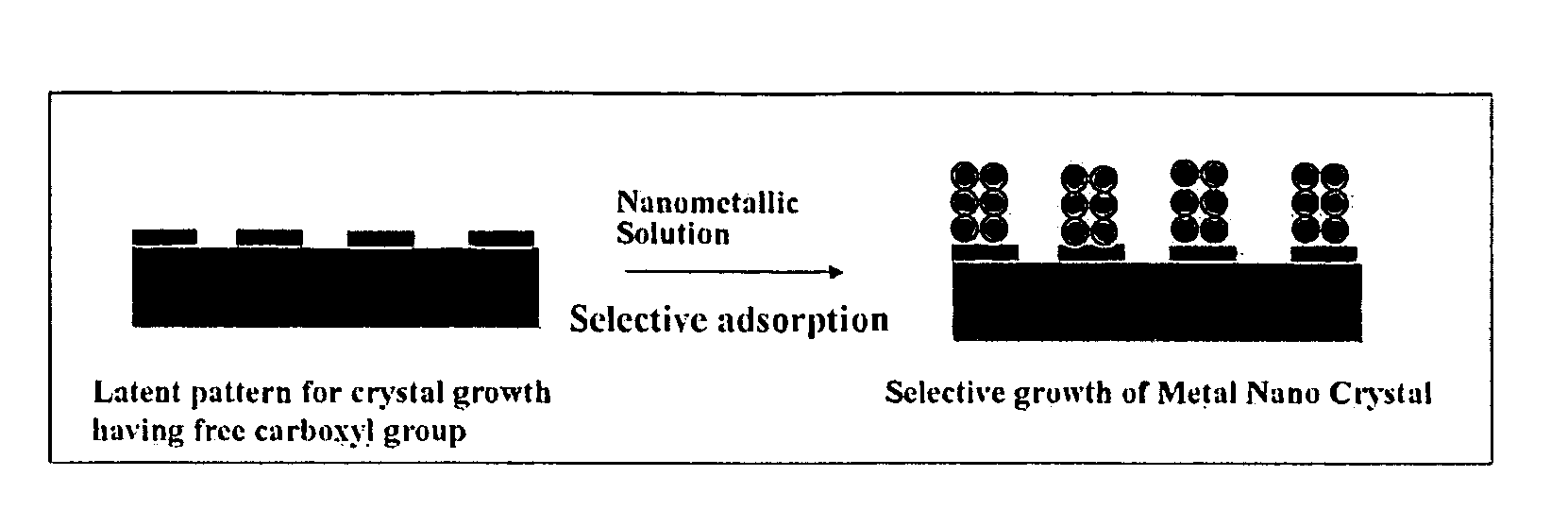
[0048]1–1) Formation of Latent Pattern for Crystal Growth Having Carboxyl Group

[0049]1 g of poly(t-butylmethacrylate-co-2-hydroxyethylmethacrylate) copolymer (Formula 3) was dissolved in 10 g of propylene glycol monomethyl ethyl acetate (PGMEA) as a solvent, and then the solution was spin-coated on a transparent polyester film. The coated film was dried at 100° C. for 10 minutes to prepare a photosensitive film having a thickness of about 100 nm. UV light was irradiated from a UV exposure system (Oriel, U.S.A) to the photosensitive film through a photomask on which a minute pattern was formed in the presence of the onium salt of Formula 2 as a photoacid generator. The exposed film was subjected to post exposure baking by heating to 120° C. for 10 minutes, and developed with pure water to form a latent pattern for crystal growth having an exposed free carboxyl group, on which a metal pattern could be formed.

[0050]

[0051]1-2) Formation of Metal Pattern Consisting of Nanocrystals;

[0052]...

example 2

[0053]The substrate prepared in Example 1-1) was dipped in a composition for metal crystal growth consisting of 16.9 g of AgNO3, 12.5 g of NH4OH, 1.2 g of C4H4O6KNa and 20 g of H2O for 10 minutes to grow crystals of a patterned metal wiring. The above procedure was repeated once to form a wiring pattern of silver. The conductivity of the patterned substrate is shown in Table 2. The conductivity was measured by the same method as in Example 1.

example 3

[0054]The substrate prepared in Example 1-1) was dipped in a composition for metal crystal growth consisting of 16.9 g of AgNO3, 12.5 g of NH4OH, 1.2 g of C4H4O6KNa and 40 g of H2O for one minute to grow crystals of a patterned metal wiring. The above procedure was repeated three times to form a wiring pattern of silver. The conductivity of the patterned substrate is shown in Table 2. The conductivity was measured by the same method as in Example 1.


PUM


Abstract

Disclosed herein is a method for forming a metal pattern by using metal nanocrystals. The method comprises the steps of: (i) coating a photosensitive compound having a substituent, which is converted into a free carboxyl group by light exposure, on a substrate to form a photosensitive film; (ii) selectively exposing the photosensitive film to light in the presence of a photoacid generator to form a latent pattern for crystal growth having a free carboxyl group; and (iii) treating the latent pattern for crystal growth with a nanometallic solution in which metal nanocrystals can be formed to grow the metal nanocrystals on the latent pattern. According to the method, a metal wiring pattern can be formed in a cost-effective and relatively simple manner. Further, the metal pattern formed by the method can be useful in the manufacture of an electromagnetic interference filter for flat panel display devices or an electrode, and can thus be applied to devices, e.g., organic light-emitting devices (OLED) and organic thin-film transistors (OTFT).

Description

[0001]Priority is claimed under 35 U.S.C. § 119 to Application No. 2004-96321, filed in the Republic of Korea on Nov. 23, 2004, herein incorporated by reference.BACKGROUND OF THE INVENTION[0002]1) Field of the Invention[0003]The present invention relates to a method for forming a metal pattern by using metal nanocrystals, and more particularly to a method for forming a metal pattern by use of a photosensitive compound having a substituent, which is converted into a free carboxyl group by light exposure.[0004]2) Description of the Related Art[0005]With increasing demand for large display area and high resolution of flat panel displays, e.g., liquid crystal displays (LCD), plasma display panels (PDP), and inorganic and organic light-emitting displays (OLED), metal wirings are considerably extended in length and the design rule for the increased aperture ratio is decreased. For these reasons, there arise many problems, such as a significant increase in wiring resistance and capacitance...

Claims


Application Information

Patent Timeline
Patent Type & Authority Patents(United States)
IPC IPC(8): C23C18/30
CPCG03F7/0392G03F7/405Y10T428/31678B82B3/0057
Inventor PARK, JONG JINKIM, SANG YEOLLEE, TAE WOOPU, LYONG SUN
Owner SAMSUNG ELECTRONICS CO LTD
Why Eureka
Try Eureka