Radiation detecting apparatus, manufacturing method therefor, and radiation image pickup system

a technology of radiation detection and manufacturing method, applied in the direction of optical radiation measurement, radiation controlled devices, instruments, etc., can solve the problems of increasing noise components rather than improving, affecting the sensitivity of the former, and not achieving many improvement cases, so as to achieve high manufacturing yield and increase the sensitivity

Active Publication Date: 2007-05-08
CANON KK
View PDF20 Cites 22 Cited by
  • Summary
  • Abstract
  • Description
  • Claims
  • Application Information

AI Technical Summary

Benefits of technology

[0040]Through the above steps, the opening ratio of the radiation detecting apparatus increases, so that sensitivity can be increased. At the same time, because of a simple manufacturing process therefor, high yield in manufacturing can be attained without involving an increase in cost.

Problems solved by technology

Thus, improvement of the former affects the latter.
As a result, the improvement in sensitivity is not attained in many cases.
This would result in the increased noise components rather than the improvement because the wiring resistance or the parasitic capacitance of the signal line increases along with the miniaturization.
That is, the signal components are improved, which undesirably involves the increase in noise component.
Needless to say, when the n+ film is made thin, the resistance of the n+ film is conversely increased, with the result that the film cannot function as the PD upper electrode.
However, the a-Si film is made thick while causing the reduction in transfer ability of the switch TFT, resulting in the increase in TFT size and the decrease in opening ratio.
Also, as for the increase in the a-Si film thickness, in terms of the production problems concerning the stress thereof, the generation of the foreign matters, and the like, there is imposed the limitation.
However, the former leads to the decrease in dielectric voltage at the wiring intersections, while the latter leads to the decrease in opening ratio.
However, the former involves not only the limitations in terms of production facilities due to the increased stress, but also the limitation on increase in film thickness from the viewpoint of working.
However, the switch elements and the sensor elements are formed on the different layers, resulting in the complicated process.
Further, there arises a problem in that the number of masks increases as compared with the above case of forming the elements using the same layer.

Method used


Image

  • Radiation detecting apparatus, manufacturing method therefor, and radiation image pickup system
  • Radiation detecting apparatus, manufacturing method therefor, and radiation image pickup system
  • Radiation detecting apparatus, manufacturing method therefor, and radiation image pickup system

Examples


embodiment 1

(Embodiment 1)

[0066]First, a description will be made of an X-ray detecting apparatus using an MIS type PD in accordance with Embodiment 1.

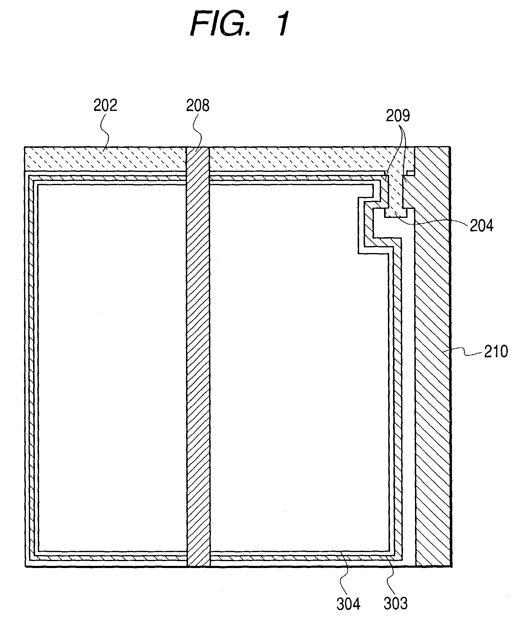
[0067]FIG. 1 is a schematic plan view showing one pixel in a case where the MIS type PD is used for a photoelectric conversion element (radiation signal conversion element). In the figure, reference numeral 202 denotes a switch TFT driving wiring; 204, a gate electrode of the switch TFT; 208, a sensor bias wiring; 210, a signal line; 209, source / drain electrodes (hereinafter, abbreviated to SD electrodes) of the switch TFT; 303, a second ohmic contact layer; and 304, a transparent electrode layer.

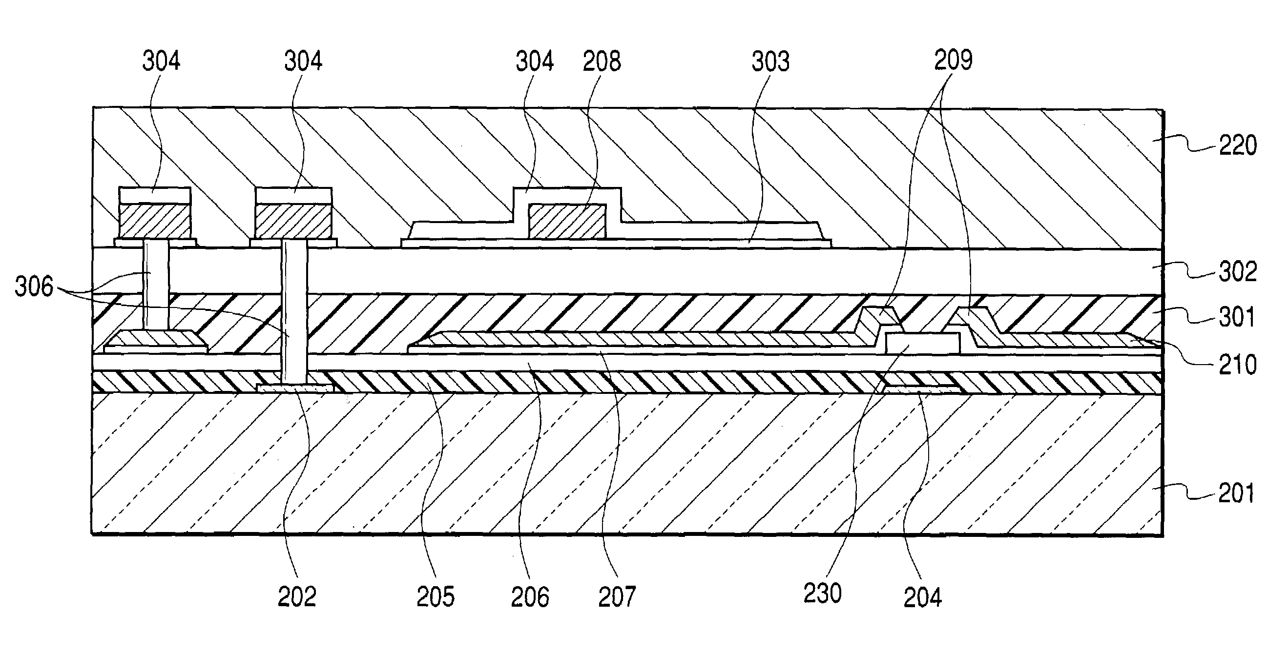
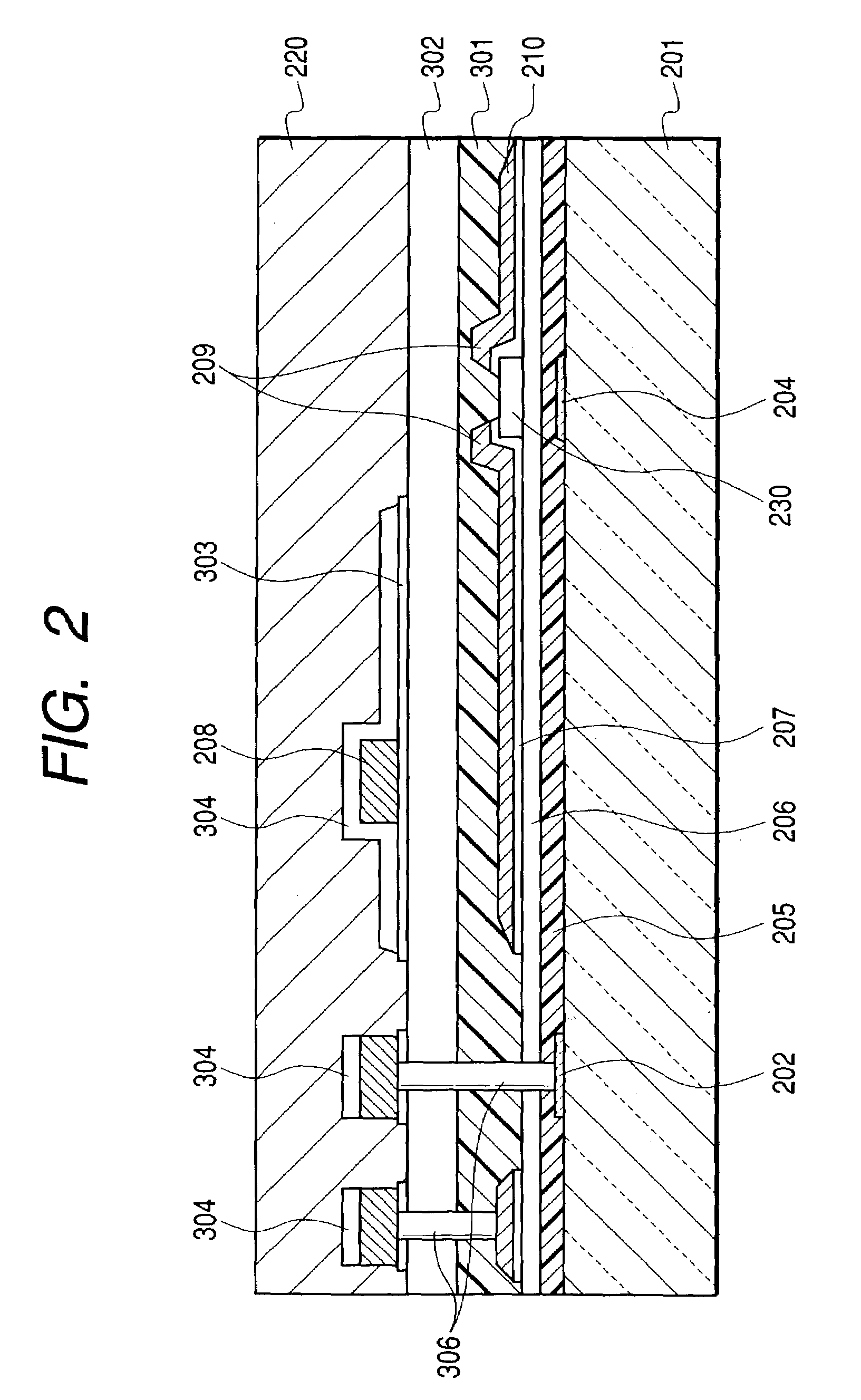
[0068]Also, FIG. 2 is a schematic sectional view showing the elements that are schematically arranged in one pixel of FIG. 1. For convenience in explanation of a manufacturing flow, a portion is also illustrated, in which the switch TFT driving wiring and the signal line are connected with a pad portion through a connection hole. In the figure, reference...

embodiment 2

(Embodiment 2)

[0086]Next, the X-ray detecting apparatus using the MIS type PD according to Embodiment 2 will be described.

[0087]FIG. 7 is a schematic plan view showing one pixel in the case of using the MIS type PD for the photoelectric conversion element. In the figure, reference numeral 202 denotes the switch TFT driving wiring; 204, the gate electrode of the switch TFT; 208, the sensor bias wiring; 210, the signal line; 209, the source / drain electrodes (hereinafter, abbreviated to SD electrodes) of the switch TFT; 303, the second ohmic contact layer; 304, the transparent electrode layer; and 305, an element isolation portion.

[0088]Also, FIG. 8 is a schematic sectional view showing the elements that are schematically arranged in one pixel of FIG. 7. In the figure, reference numeral 201 denotes the glass substrate; 202, the switch TFT driving wiring; 204, the gate electrode of the switch TFT; 205, the first gate insulating film; 206, the first intrinsic a-Si film; 203, a channel st...

embodiment 3

(Embodiment 3)

[0099]FIG. 19 is a schematic plan view showing the X-ray detecting apparatus using the MIS type PD of this embodiment. FIG. 20 is a schematic sectional view taken along the line 20—20 of FIG. 19. FIG. 21 is a schematic sectional view taken along the line 21—21 of FIG. 19.

[0100]In FIGS. 19 to 21, reference numeral 1 denotes an insulating substrate; 2, a gate electrode of a switch TFT; 3, a gate wiring connected to the gate electrode 2; 4, a first insulating layer; 5, a first semiconductor layer; 6, a first ohmic contact layer; 7, source / drain electrodes of the switch TFT; 8, a signal line connected to one of the source / drain electrodes 7; 9, a first planarization layer; 10, a contact hole; 11, a pixel electrode of the MIS type PD; 12, a second insulating layer; 13, a second semiconductor layer; 14, a second ohmic contact layer; 15, a transparent electrode layer; 16, a bias wiring of the MIS type PD; 17, a second planarization layer; 18, an adhesive layer; and 19, a phos...


PUM


Abstract

A radiation detecting apparatus having a radiation conversion element arranged on a switch TFT is provided. The apparatus includes a gate electrode of the switch TFT; a first insulating layer, a first semiconductor layer, and an ohmic contact layer, which are arranged on the gate electrode in order; and a source/drain electrode of the switch TFT arranged on the ohmic contact layer, which all constitute the switch TFT. The apparatus also includes a lower electrode of the radiation conversion element formed from the same layer as the source/drain electrode, a second insulating layer, a second semiconductor layer, and a second ohmic contact layer, which are arranged on the lower electrode in order, and a bias wiring for applying a bias voltage to the radiation conversion element.

Description

BACKGROUND OF THE INVENTION[0001]1. Field of the Invention[0002]The present invention relates to a radiation detecting apparatus for detecting a radiation such as an X-ray or a γ-ray, in particular, a radiation detecting apparatus applied to a medical imaging diagnostic apparatus, a nondestructive testing apparatus, an analyzer using the radiation, or the like and to a manufacturing method therefor.[0003]2. Related Background Art[0004]Up to now, a photographing method adopted in the field of medical imaging diagnosis has been generally classified into ordinary photographing for obtaining a still image and fluorography for obtaining a moving image. The respective photographing methods are selected while taking into consideration a photographing apparatus as needed.[0005]In recent years, along with progress in liquid crystal TFT technology and improvement in information (hereinafter, abbreviated to FPD) has been proposed, which includes: a sensor array composed of a photoelectric conv...

Claims


Application Information

Patent Timeline
Patent Type & Authority Patents(United States)
IPC IPC(8): G01J1/00G01T1/24H01L27/146
CPCH01L27/14609H01L27/14676H01L27/14692
Inventor NOMURA, KEIICHIMORISHITA, MASAKAZUMOCHIZUKI, CHIORI
Owner CANON KK
Why Eureka
Try Eureka