Method and apparatus for inspecting pattern defects

a pattern defect and inspection method technology, applied in the direction of optically investigating flaws/contamination, semiconductor/solid-state device testing/measurement, instruments, etc., can solve the problems of low lighting efficiency, large size, and difficulty in correcting the chromatic aberration of the optical system used for pattern inspection, and achieve high reliability, resolution and stability. high

Inactive Publication Date: 2007-05-15
HITACHI LTD
View PDF10 Cites 24 Cited by
  • Summary
  • Abstract
  • Description
  • Claims
  • Application Information

AI Technical Summary

Benefits of technology

[0013]The present invention has the object of eliminating the aforesaid problems and providing a highly reliable pattern defect inspection me...

Problems solved by technology

A larger size lamp with higher power must be used to obtain a high intensity sufficient for high-speed pattern inspection, but this results in the problem of lower lighting efficiency.
Even if high intensity illumination is obtained by utilizing a wider spectral band, there is the problem that correcting the chromatic aberration of optical systems used for pattern inspecti...

Method used


Image

  • Method and apparatus for inspecting pattern defects
  • Method and apparatus for inspecting pattern defects
  • Method and apparatus for inspecting pattern defects

Examples


first embodiment

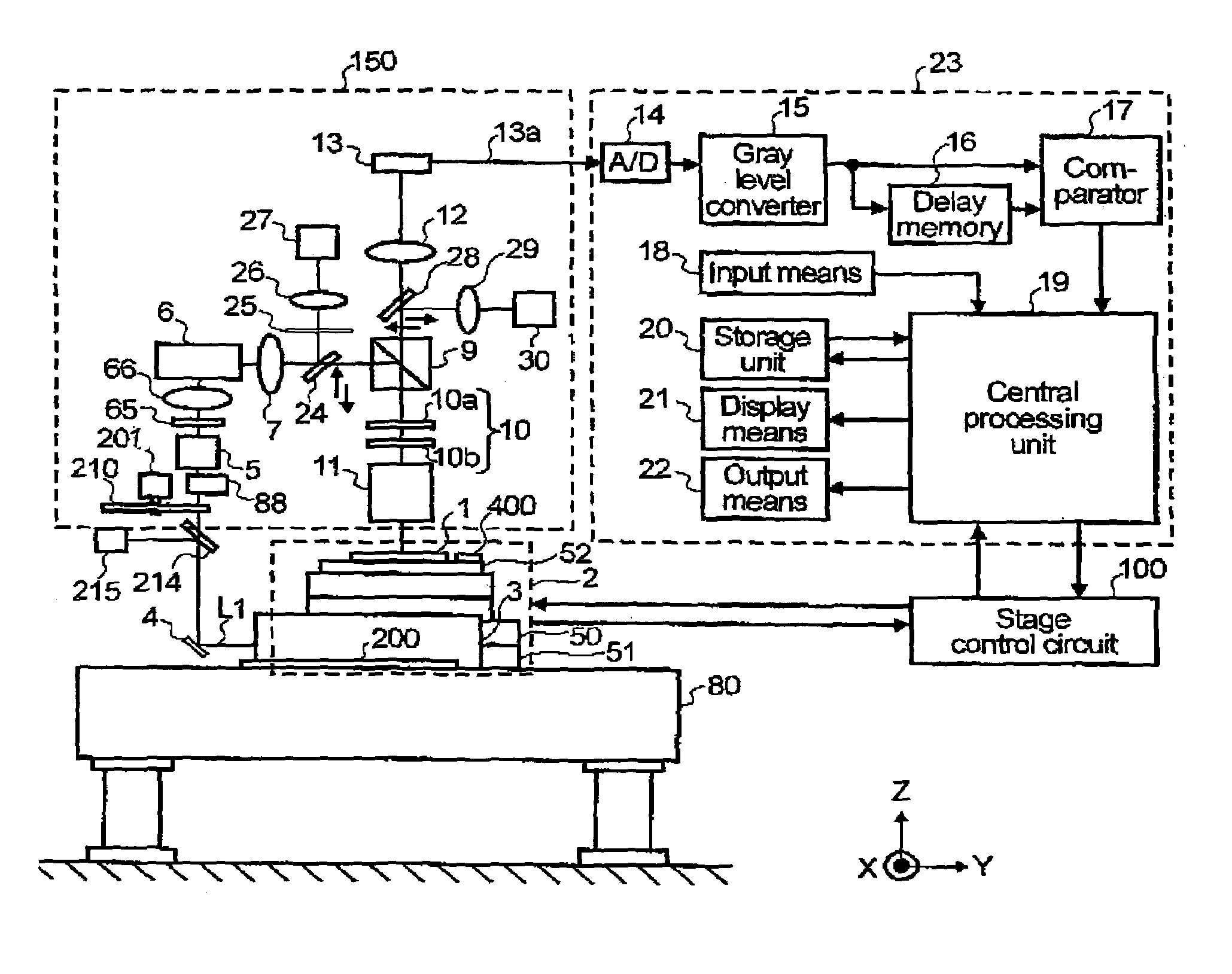
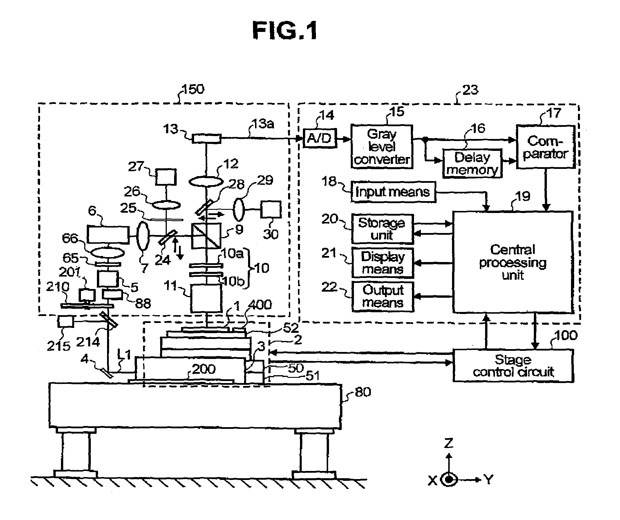
[0036]FIG. 1 is a schematic diagram showing a pattern defect inspection apparatus representing the present invention. A sample 1 comprised of a semiconductor wafer (device under test), on which there is fabricated a circuit pattern to be inspected, is placed on a stage 2. The stage 2 consists of a Z stage 52 that moves in the Z direction and rotates, a Y stage 51, an X stage 50, and a position measurement device (not shown in drawing) that measures the position of each stage. Each stage can be moved to any desired position under control from a stage controller circuit 100 that is connected to a central processing unit 19.

[0037]Component 3 in FIG. 1 is an ultraviolet laser light source (ultraviolet laser generator) that emits a far ultraviolet laser beam so as to illuminate the sample with far ultraviolet light of high intensity. A laser beam L1, that is emitted from the ultraviolet laser light source 3, is reflected from a mirror 4 and enters an objective lens 11 by way of a density...

second embodiment

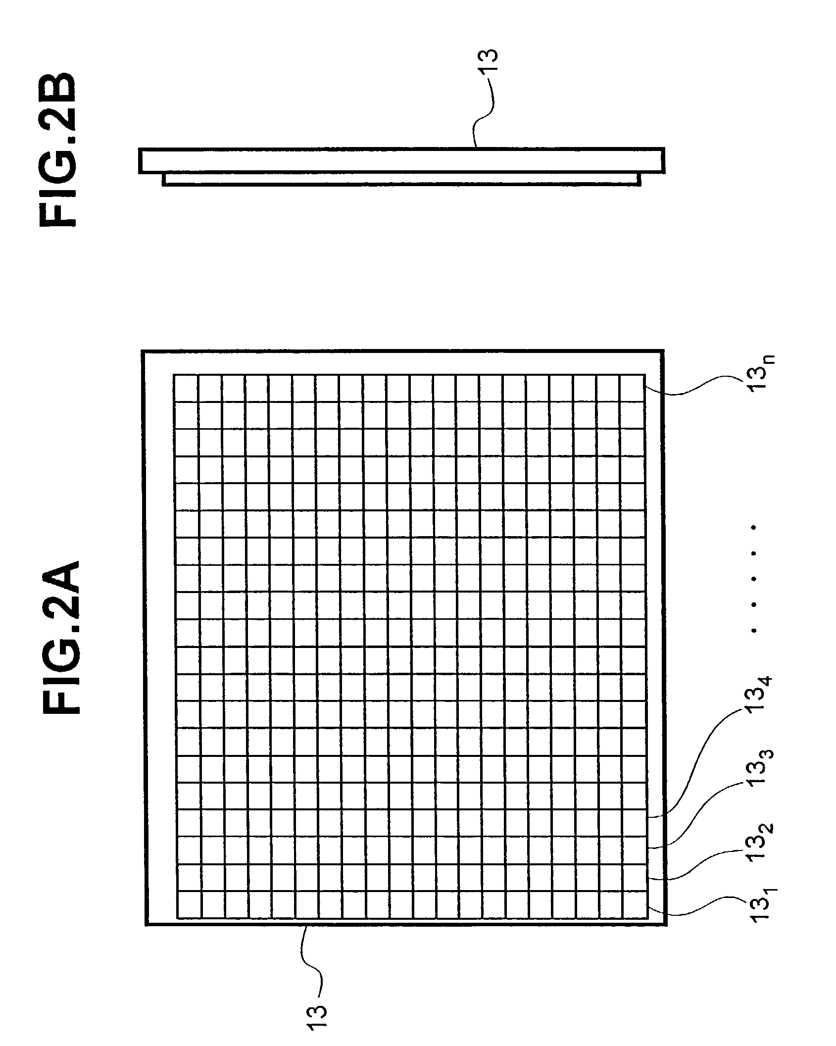
[0057]As the present invention, the laser beam L1 may be input into the objective lens, while changing the irradiance of the laser beam L1 according to the scan track of the laser beam L1 on the pupil 11a of the objective lens 11. More specifically, the scan track of the laser beam L1 is detected in advance, by way of the screen 25, lens 26 and TV camera 27, so as to measure the positional relation with the drive signal fed to the motors 61 and 64 that scan the laser beam L1. The irradiance of the laser beam L1 is then controlled at high speeds by using a density adjustment means 88, as shown in FIG. 1. An optical element, such as an A / O modulator, can be used as the density adjustment means 88.

[0058]In accordance with the present invention, the cycle of the two-dimensional scan of the laser beam L1 is synchronized with the image acquisition cycle of the image sensor 13, and the incident angle θ of the light beam is also sequentially changed according to each cycle. This allows imag...


PUM


Abstract

A pattern defect inspection apparatus is capable of detecting defects, without being affected by non-uniform thickness of a thin film formed on a sample, even when using monochromatic light, such as a laser. The apparatus comprises a laser to illuminate a sample, coherence suppression optics to reduce laser beam coherence, a condenser to condense the laser beam onto a pupil plane of an objective lens, and a detector to detect the light reflected from a circuit pattern formed on a sample. The condenser is designed so that the intensity of light illuminating the sample under test can be partially adjusted according to the type of laser beam illumination condensed on the pupil of the objective lens. Variations in reflected light intensity caused by non-uniform film thickness on the surface of the sample are therefore reduced, and shading is minimized in the detected image to allow detecting of fine defects.

Description

BACKGROUND OF THE INVENTION[0001]The present invention relates to pattern defect inspection methods and apparatus using a laser beam as illumination light, mainly for inspecting and observing defects of micro patterns or foreign matter contamination occurring in manufacturing processes for semiconductor devices and flat panel displays.[0002]Circuit patterns tend to become finer and smaller as semiconductor devices become more highly integrated. Smaller and finer circuit patterns have spurred a demand for higher resolution when inspecting for defects of circuit patterns that have been formed on semiconductor wafers by photolithographic processes using photomasks or reticles. One technique for enhancing resolution when detecting pattern defects involves the use of illumination light on shorter wavelengths from visible light to ultraviolet light. Mercury lamps and xenon lamps, for example, have been conventionally used as illumination light sources, while only the required wavelengths ...

Claims


Application Information

Patent Timeline
IPC IPC(8): G01N21/00G01B11/30G01N21/94G01N21/95G01N21/956H01L21/66
CPCG01N21/94G01N21/956G01N2021/9513G01N2201/10G01N2201/1045
Inventor UTO, SACHIOYOSHIDA, MINORUNAKATA, TOSHIHIKOMAEDA, SHUNJI
Owner HITACHI LTD
Why Eureka
Try Eureka