Method for producing a conducting doped diamond-like nanocomposite film and a conducting doped diamond-like nanocomposite film

Inactive Publication Date: 2007-05-29
INT TECH EXCHANGE
View PDF4 Cites 6 Cited by
  • Summary
  • Abstract
  • Description
  • Claims
  • Application Information

AI Technical Summary

Benefits of technology

[0019]Diamond-like nanocomposite materials have a wide range of applications as thermoresistive films, infrared light emitting films and protective c

Problems solved by technology

This conventional method for producing a metal-doped diamond-like nanocomposite film has significant deficiencies.
Moreover, the clustering of the film results in instability of the metastable nanostructure with weak chemical links when the film is heated in use to higher temperatures.
For the aforementioned reasons, instability of the film microstructure is already seen at a temperature of about 600° C., and this is accompanied by a temperature and time instability of electrical resistance of the film.
The method for producing the film does not guarantee, due to its complexity, one-to-one reproduction of atomic concentrations of the elements contained in the film.
Reduction in the carbon concentration leads to loss of the diamond-like properties and decreases the percent yield of films with diamond-like properties of the total quantity of the produced films.
The diamond-like films produced by the above method and having an atomic concentration of carbon of about 40% and an atomic concentration of metal of 20-2

Method used


Image

  • Method for producing a conducting doped diamond-like nanocomposite film and a conducting doped diamond-like nanocomposite film
  • Method for producing a conducting doped diamond-like nanocomposite film and a conducting doped diamond-like nanocomposite film
  • Method for producing a conducting doped diamond-like nanocomposite film and a conducting doped diamond-like nanocomposite film

Examples


Embodiment Construction

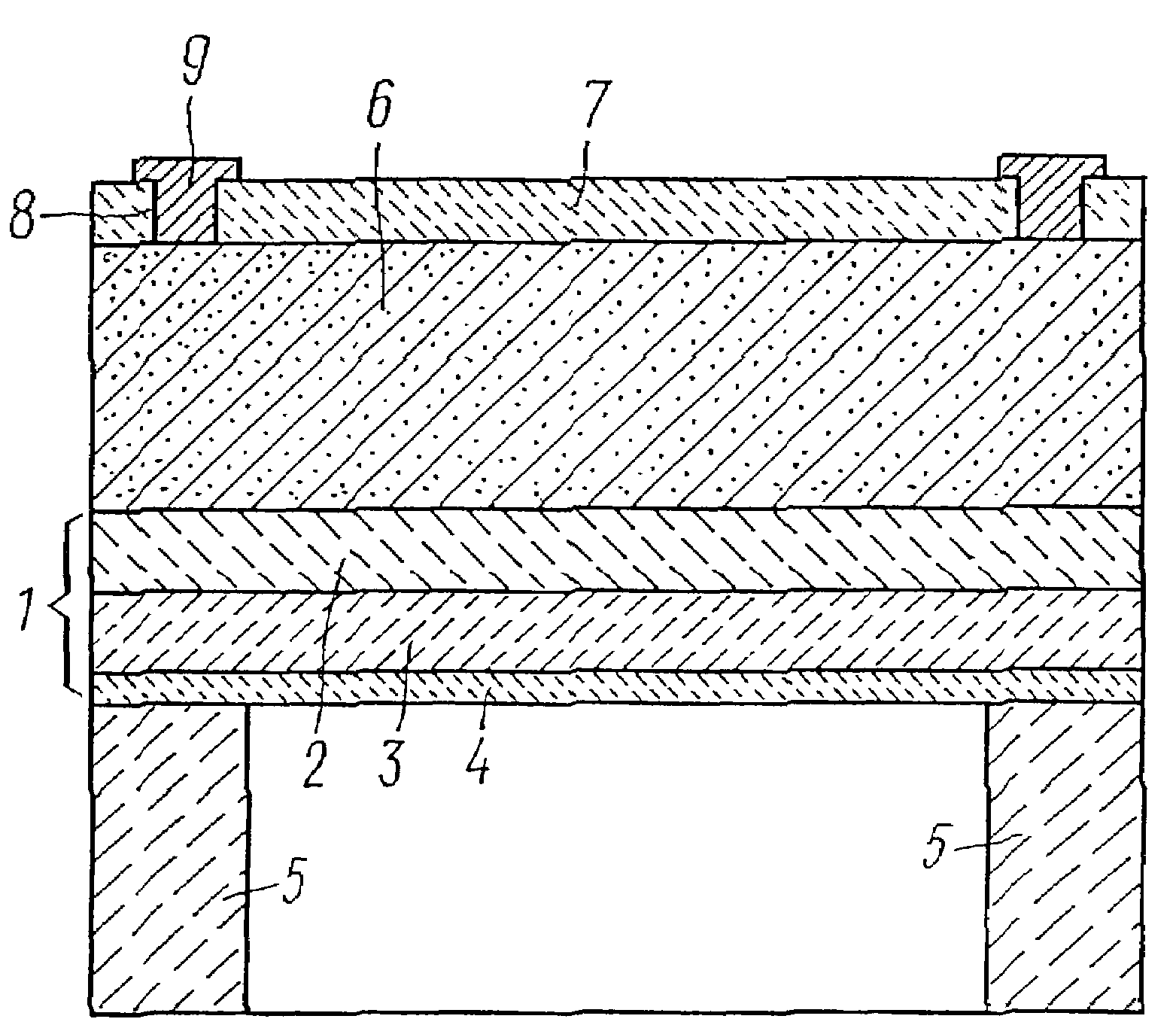
[0024]The new class of doped diamond-like nanocomposites of the invention has an amorphous anisotropic layered structure which exhibits a high degree of thermal stability, high electrical conductivity combined with heat resistance, mechanical strength at thermal cycling, and stable electrical properties. The diamond-like nanocomposites contain, as basic elements, carbon, silicon, oxygen and hydrogen and metal as a dopant.

[0025]The conducting doped diamond-like nanocomposite film is produced in the following manner: A holder with a substrate of a dielectric material, having a thickness in the range from 1 to 10 microns is disposed in a vacuum chamber. A voltage of 0.3-5.0 kV with a frequency within the range from 1 to 25 MHz is applied to the substrate holder, and the temperature of the substrate is maintained within the range from 200 to 500° C. A gas discharge plasma with an energy density greater than 5 kilowatt-hour / gram-atom of carbon particles is generated in the vacuum chamber...


PUM

PropertyMeasurementUnit
Temperatureaaaaaaaaaa

Abstract

The present invention provides a method for producing a conducting doped diamond-like nanocomposite film containing, as basic elements, carbon, silicon, metal, oxygen and hydrogen. The film is produced as follows: a substrate is disposed in a vacuum chamber, and a voltage of 0.3-5.0 kV is applied to the substrate; a gas discharge plasma with an energy density of more than 5 kilowatt-hour/gram-atom of carbon particles is generated, and an organosiloxane compound is evaporated into the plasma; a beam of particles of a dopant is introduced into the plasma; and a film is grown on the substrate to produce a conducting doped carbon nanocomposite film with a predetermined relationship of atomic concentrations of carbon, metal and silicon. The film surface is coated with a silicon dioxide layer. A unidirectional alternating current is passed through the film in a current generator mode to effect electric thermal exposure of the film. As the result, a conducting doped diamond-like nanocomposite film having a multilayer structure is produced.

Description

RELATED APPLICATION[0001]This application is related to PCT Patent Application No. PCT / RU01 / 00058, filed 8 Feb. 2001, the disclosure of which is incorporated by reference in its entirety for all purposes.TECHNICAL FIELD[0002]The present invention relates to microelectronics and more specifically to a method for producing a conducting doped diamond-like nanocomposite film and to such a conducting doped diamond-like nanocomposite film.[0003]The films are applicable in microelectronics as resistors, which emit infrared light when heated by a current, and can be used in spectroscopic instruments, gas detectors and thermal printers.BACKGROUND[0004]A method for producing a conducting metal-containing diamond-like nanocomposite film containing, as basic elements, carbon, silicon, metal, oxygen and hydrogen, and disposed on a dielectric substrate is known from U.S. Pat. No. 5,352,493. The method for producing the film is the following: A holder with a substrate of a dielectric material is p...

Claims


Application Information

Patent Timeline
IPC IPC(8): C23C16/26C23C16/27C23C16/30C23C16/46C23C30/00
CPCC23C16/30Y10T428/30Y10T428/265
Inventor SIDOROVA, LJUDMILA PETROVNADMITRIEV, VITALY KONSTANTINOVICHINKIN, VITALY NIKOLAEVICH
Owner INT TECH EXCHANGE
Why Eureka
Try Eureka