Time resolved non-invasive diagnostics system

a diagnostic system and time resolution technology, applied in the field of time resolution non-invasive diagnostic systems, can solve the problems of multiple levels of metal interconnects, time-consuming and destructive methods, and inability to locate failures of semiconductor devices, so as to improve light collection efficiency and imaging resolution, and enhance system stability.

Inactive Publication Date: 2007-05-29
DCG SYST
View PDF19 Cites 31 Cited by
  • Summary
  • Abstract
  • Description
  • Claims
  • Application Information

AI Technical Summary

Benefits of technology

[0029]In another aspect of the invention, the inventive system comprises an x-y-z stage that is used to move the optics to the location of interest on the device under test, and focus and image the device(s) of interest. The navigation is performed in relation to a CAD layout of the IC. A mechanized shutter is used to variably define imaging areas within the field of view of the optics. During navigation and target acquisition, the device is illuminated and is imaged with an image intensifier, thereby providing high spatial resolution. When a device to be tested has been acquired, i.e., placed within the imaging area, the illumination source is turned off and the device is stimulated with test signals. During the stimulation period, hot electron photoemission is collected by the optics and is imaged onto a fiber optics.
[0030]To provide the temporal resolution, emission detection is synchronized with the test signals, i.e., the automated test equipment (ATE). Light collected by the fiber optics is detected by an avalanche photodiode (APD), which is coupled to an avalanche quenching circuit, a time-to-amplitude converter (TAC), and a multi-channel analyzer. Optionally, the APD is gated so that it assumes the detection condition only just before a light emission is expected according to the sync signal from the ATE. This provides reduction in noise and increases the life of the APD.
[0032]According to a particular feature of the invention, an immersion lens is used to increase the light collection efficiency and imaging resolution. In one inventive embodiment, the index matched immersion lens is bi-convex and is pressured onto the DUT during emission detection to ensure direct (no air-gap) contact with the DUT.
[0033]An autofocus may also be provided for enhanced stability of the system. According to one embodiment, the autofocus is a passive system, i.e., includes no illumination source, but rather uses a feedback loop optimizing the collection rate of the photoemission light.

Problems solved by technology

For example, avalanche breakdown in insulators cause light emission, and detection of such light emission can point to the locations of failure in the device.
Various emission microscopes have been used for detecting locations on the device where the electrical current drawn exceeds the expected levels and therefore could lead to locating failures in semiconductor devices.
One problem in probing flip chip packaged devices using conventional dynamic (timing) diagnostic methods, such as e-beam (voltage-contrast) probing, is that the critical nodes where timing information and fault isolation is critical are not readily accessible and masked by multiple levels of metal interconnects.
The former is a time consuming and destructive method, and the latter wastes precious “real-estate” and in many cases does not represent the features of interest to the circuit designer.
However, in spite of the amount of work in the field, there is still no commercially viable system for device debug by time resolved measurements of hot electron emission.

Method used


Image

  • Time resolved non-invasive diagnostics system
  • Time resolved non-invasive diagnostics system
  • Time resolved non-invasive diagnostics system

Examples


Embodiment Construction

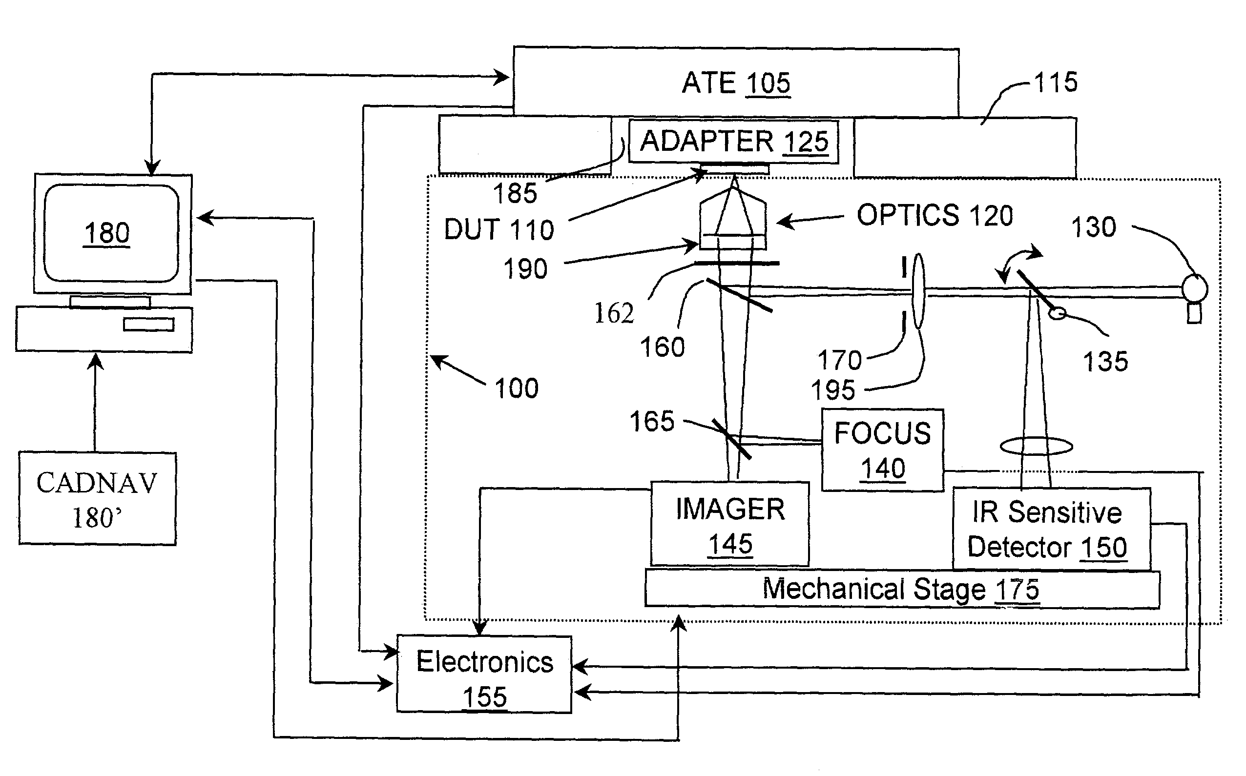
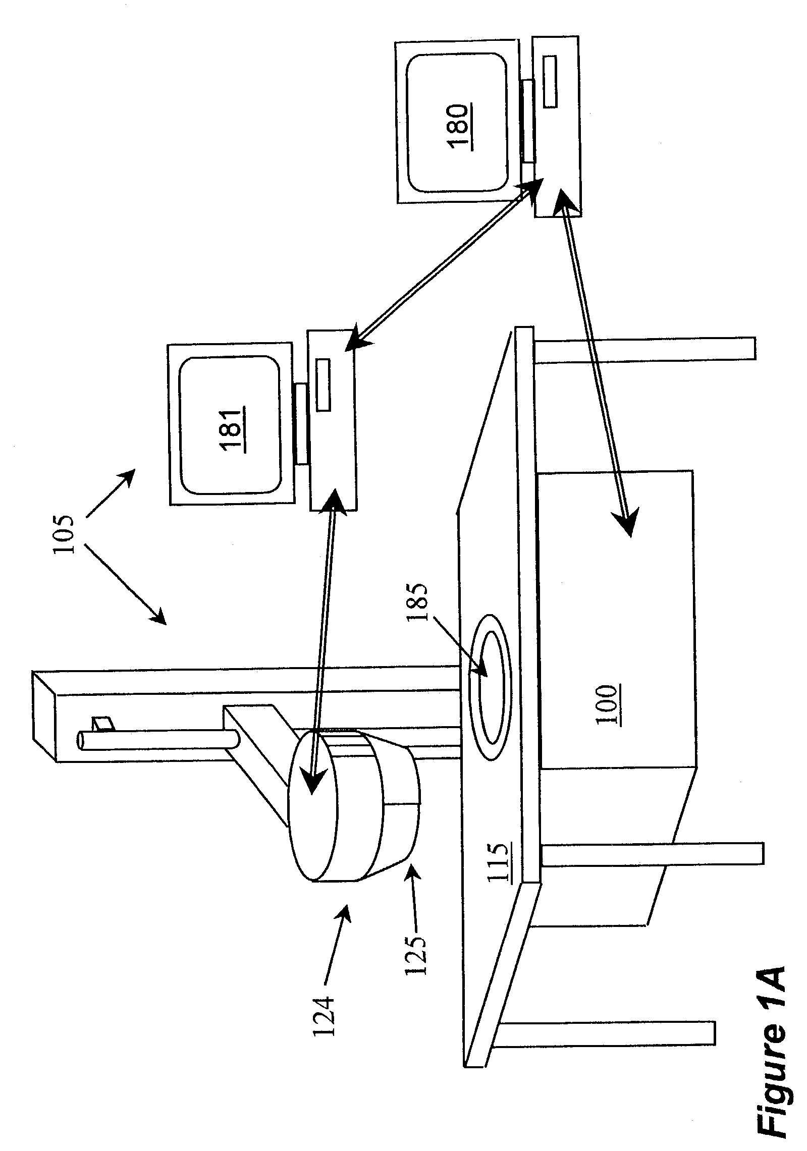
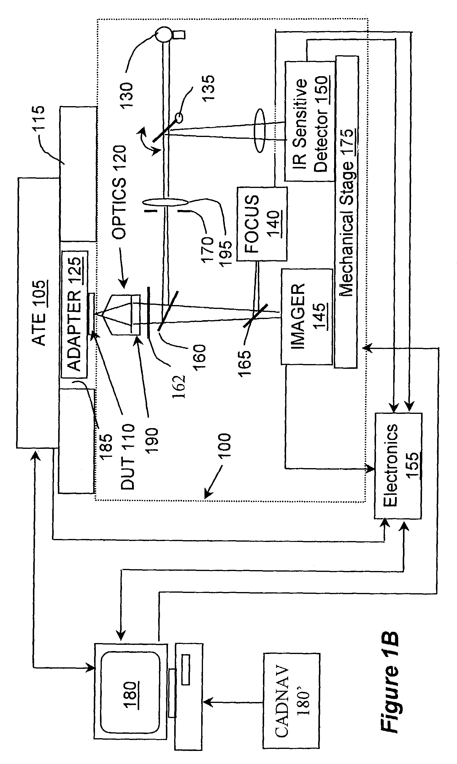
[0048]The present invention provides a testing system particularly suitable for rise time, timing; logic fault localization and other testing of microchips, especially from the backside through the substrate (e.g., flip chip packaged devices). Accordingly, the description proceeds with examples using flip chip. However, it should be appreciated that the invention is not limited to testing flip chips. For example, it is possible to take top-side packaged devices and “flip” them in a chip-scale package (CSP), or design the proper opening to ensure the emitted light gets through the top-side. What is desired is to be able to collect emission from a device of interest in the chip.

[0049]FIGS. 1A and 1B are general schematics depicting the major components of the testing and debug system according to an exemplary embodiment of the invention. The system operates in conjunction with a commercially available automated testing equipment 105 (ATE). The ATE generally comprises a controller, suc...


PUM


Abstract

A system for probe-less non-invasive detection of electrical signals from integrated circuit devices is disclosed. The system includes an illumination source, collection optics, imaging optics, and a photon sensor. In a navigation mode, the light source is activated and the imaging optics is used to identify the target area on the chip and appropriately position the collection optics. Once the collection optics is appropriately positioned, the light source is deactivated and the photon sensor is used to detect photons emitted from the chip. No mention of cooling (active device measurement capability) and advanced optics to detect the features (SIL).

Description

[0001]This application is a divisional of, and claims priority from, U.S. patent application Ser. No. 09 / 995,548, filed Nov. 28, 2001 now U.S. Pat No. 6,621,275.BACKGROUND OF THE INVENTION[0002]1. Field of the Invention[0003]The present invention relates to a system for in-situ transistor level measurement of circuit timing information directly related to the switching events (logic transitions) of switching events of transistors of electrically active semiconductor integrated circuits.[0004]2. Description of the Related Art[0005]It is known in the prior art that various mechanisms in semiconductor devices can cause light emission. Detection of such light emission has been used to investigate semiconductor devices. For example, avalanche breakdown in insulators cause light emission, and detection of such light emission can point to the locations of failure in the device. Similar detection can be used to characterize electrostatic discharge in the device. In electrically stimulated (...

Claims


Application Information

Patent Timeline
Patent Type & Authority Patents(United States)
IPC IPC(8): G06K9/00G01R31/28G01R31/311
CPCG01R31/311G01N21/84
Inventor COTTON, DANIEL MURDOCHPAKDAMAN, NADERVICKERS, JAMES SQUIREWONG, THOMAS
Owner DCG SYST
Why Eureka
Try Eureka