Display system

a display system and display technology, applied in the field of display systems, can solve the problems of poor connection, increase of wiring resistance of the connection portion, increase of the area of the peripheral portion, etc., and achieve the effect of low power consumption

Inactive Publication Date: 2007-06-12
SEMICON ENERGY LAB CO LTD
View PDF15 Cites 65 Cited by
  • Summary
  • Abstract
  • Description
  • Claims
  • Application Information

AI Technical Summary

Benefits of technology

[0032]In view of the above, an object of the present invention is to solve a problem with respect to a wiring capacitance in a connection portion which occurs when bonding a memory and control circuits, to thereby provide a display system with low power consumption.

Problems solved by technology

However, as described above, when the driver circuits are incorporated into the display system, an increase in a wiring resistance of the connection portion, poor connection thereof, an increase of an area of a peripheral portion (frame region) of a pixel portion, and the like become problems.
Here, in the case of the a-TFT, there is a problem such as small field effect mobility.
Thus, in the case of driver circuits using the a-TFT, there is a problem that a frequency characteristic cannot be improved.
Thus, when connecting the memory and the control circuits onto the display substrate, a wiring capacitance in the connection portion becomes a problem.
Since wiring capacitances in the connection portions between the respective driver circuits and the pixel portion which are formed on the display substrate, and the memory and the control circuits which are externally attached thereto, are increased, the power consumption of the entire display system cannot be reduced.

Method used


Image

  • Display system
  • Display system
  • Display system

Examples


embodiment 1

[Embodiment 1]

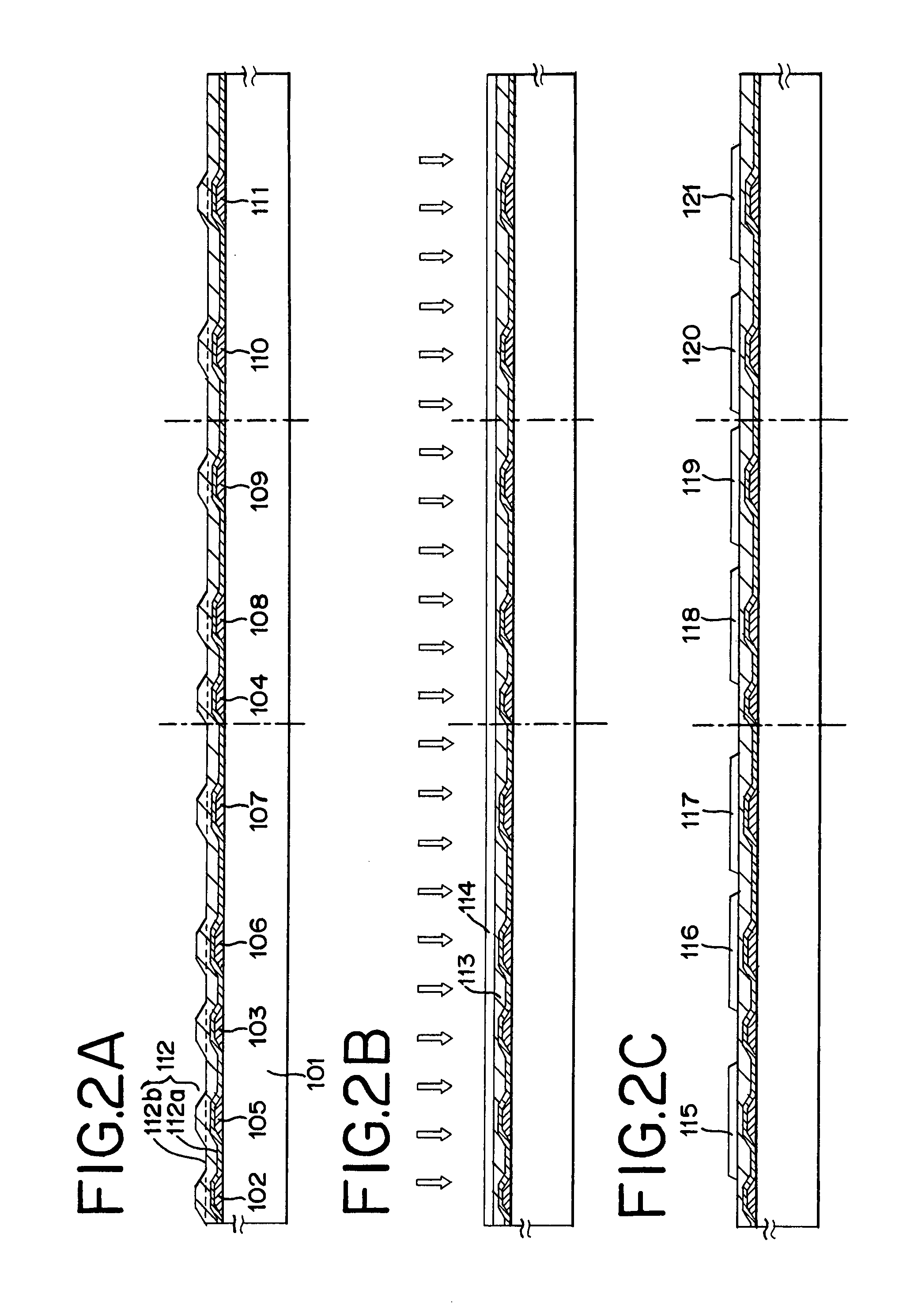
[0184]Manufacturing steps of manufacturing a displaying system according to the present invention will be described. In this embodiment, a method of simultaneously manufacturing TFTs (typically shown a switching TFT and a driving TFT in the figure) for a pixel portion, TFTs (an n-channel type TFTs and an p-channel type TFTs) for each driver circuit (a source signal line driver circuit and a gate signal line driver circuit) and TFTs (an writing TFT and an n-channel type TFT and a p-channel type TFT constituting the first inverter which are shown typically) on the same substrate will be described in detail.

[0185]In this embodiment, an example in which a common voltage is applied to the first electrodes of all the TFTs formed on the pixel portion and the first electrode is connected to the second electrode of each TFT formed on the driver circuit is shown. FIGS. 2A to 6 are cross-sectional views for explaining manufacturing steps.

[0186]In FIG. 2A, a substrate made of an a...

embodiment 2

[Embodiment 2]

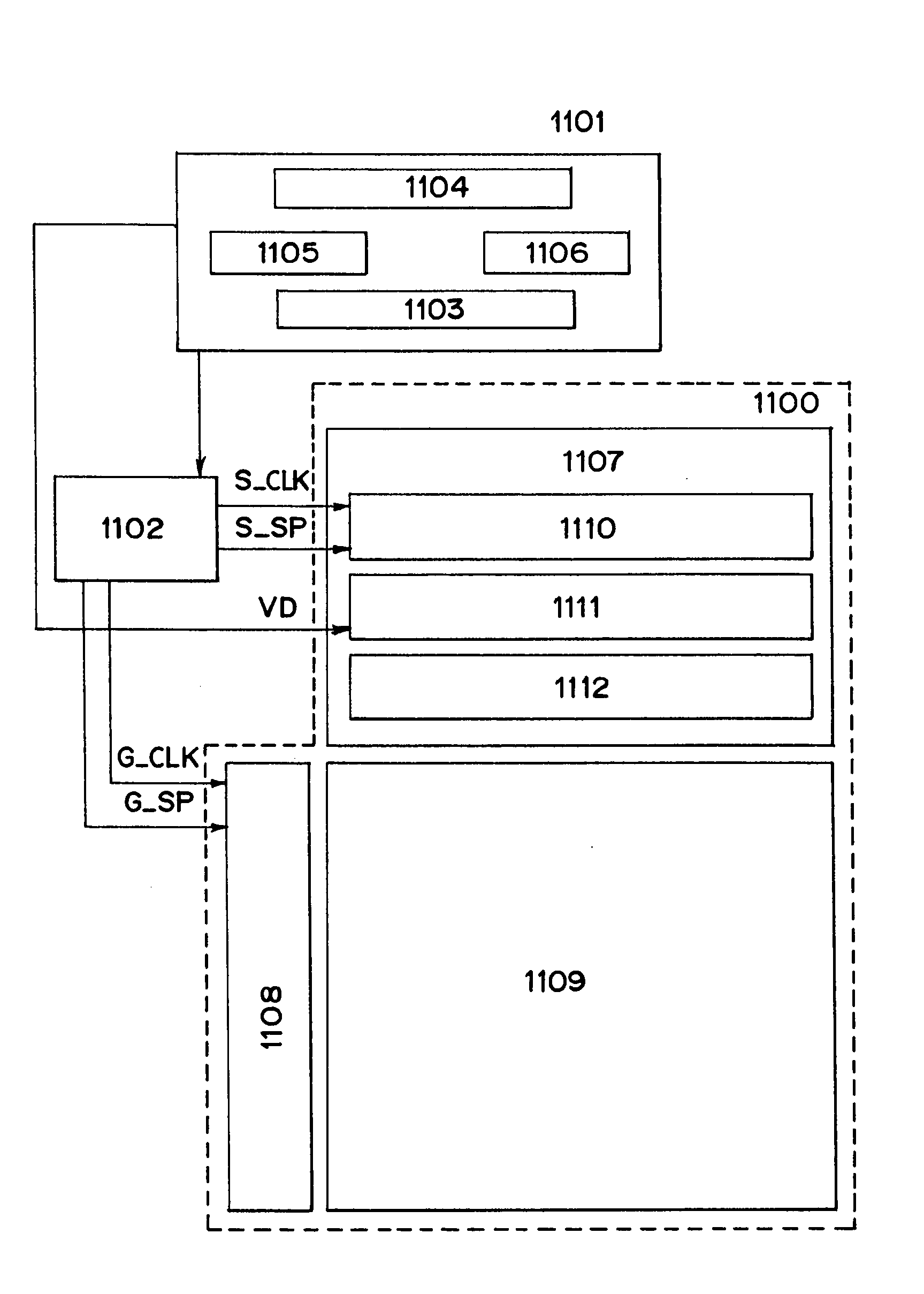
[0226]In this embodiment, the different configuration of the display system from Embodiment 1 will be described.

[0227]FIG. 7 is a cross-sectional view of pixels of the display system in this embodiment.

[0228]Reference symbol 501 denotes an n-channel type TFT, which functions as a switching TFT, and 502 denotes a p-channel type TFT, which functions as a driving TFT. The switching TFT 501 includes a semiconductor film 553, a first insulating film 507 (507a and 507b), first electrode 505, a second insulating film 513, and second electrode 514. The semiconductor film 553 includes a first concentration impurity region 508 (508a and 508b), a second concentration impurity region 509 (509a and 509b) and channel-forming region 510.

[0229]The first electrode 505 is overlapped with the channel-forming region 510 with the fist insulating film 507 put therebetween. In addition, the second electrode 514 is overlapped with the channel-forming region 510 with the second insulating film...

embodiment 3

[Embodiment 3]

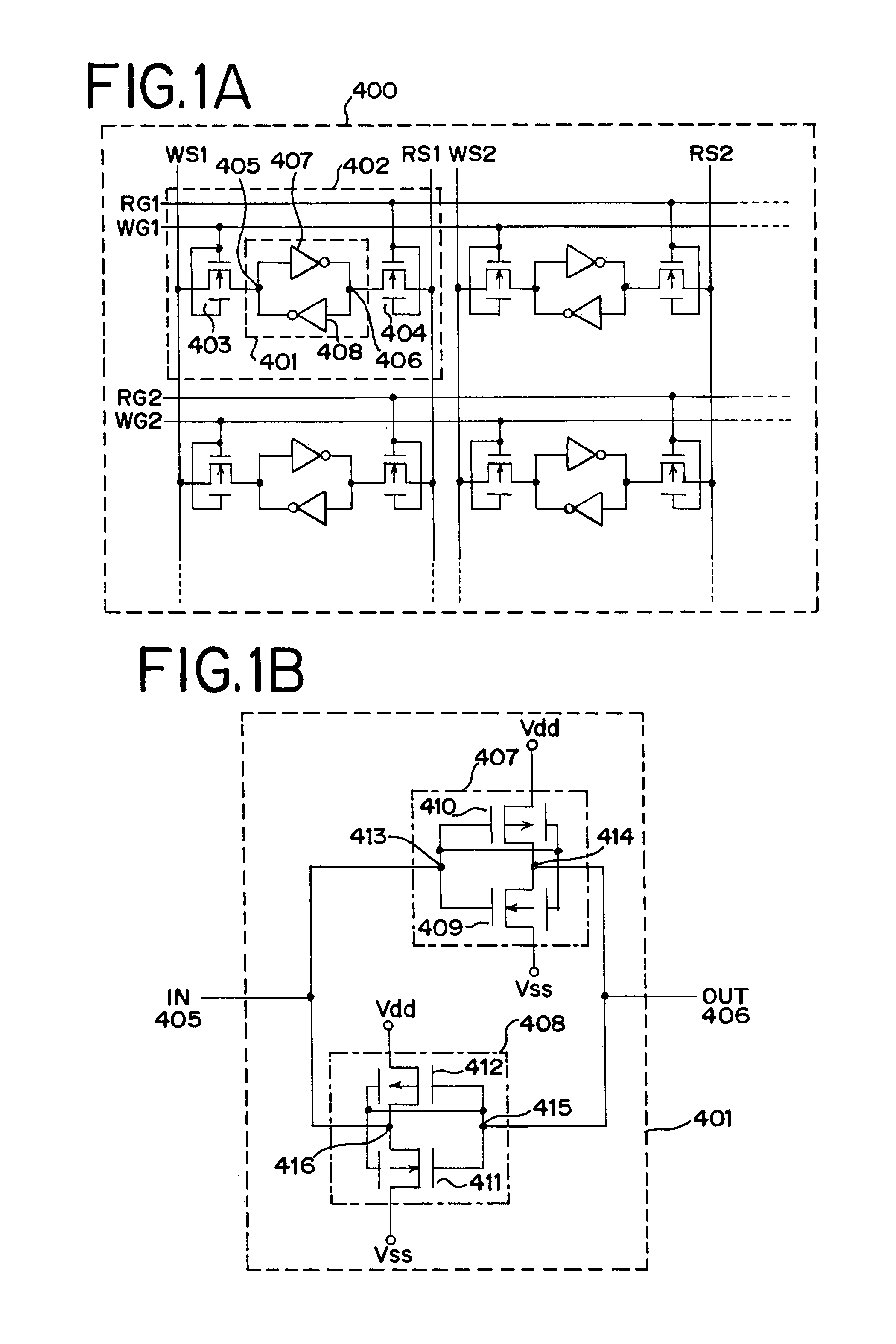
[0236]In this embodiment, a flip-flop circuit used for the shift register of a driver circuit will be described while taking a case of forming a TFT having a first electrode and a second electrode electrically connected to each other, as an example.

[0237]FIGS. 8A and 8B are circuit diagrams of a flip-flop circuit in this embodiment. The configuration of the flip-flop circuit included in the display system of the present invention is not limited to that shown in FIGS. 8A and 8B. In addition, the flip-flop circuit is only one example of the circuits included in the driver circuit. It does not necessarily mean that the display system of the present invention includes a flip-flop circuit.

[0238]The flip-flop circuit shown in FIG. 8A includes clocked inverters 1401 and 1402 and an inverter 1403. FIG. 8B is a circuit diagram which shows the respective circuit elements of the flip-flop circuit shown in FIG. 8A more concretely.

[0239]Each of the clocked inverters (1401 and 1402)...


PUM

PropertyMeasurementUnit
thicknessaaaaaaaaaa
thicknessaaaaaaaaaa
thicknessaaaaaaaaaa

Abstract

To solve a problem of increased power consumption power due to wiring capacitances, which occurs when connecting onto a display substrate a substrate on which a memory, a memory controller, and the like are formed. The memory, the memory controller, and the like are integrally formed on the display substrate. At this time, these circuits are formed using a dual gate TFT. Thus, a display device in which wiring capacitances of connection portions between driver circuits composing a display and the memory controller and the like are reduced and which has thus low power consumption can be provided.

Description

BACKGROUND OF THE INVENTION[0001]1. Field of the Invention[0002]The present invention relates to a display system for displaying an image by inputting a digital video signal. Also, the present invention relates to an electronic device using the display system.[0003]2. Description of the Related Art[0004]A display system in which light emitting elements are arranged in respective pixels and light emission of the light emitting elements is controlled to display an image will be described below.[0005]Here, an example in the case where a light emitting device is an element (OLED element) having a structure in which an organic compound layer for producing light emission upon generation of an electric field is sandwiched between an anode and a cathode will be described. Also, the light emitting element indicates both an element using light emission produced at transition from a singlet exciton to a ground state (fluorescence) and an element using light emission produced at transition from...

Claims


Application Information

Patent Timeline
Patent Type & Authority Patents(United States)
IPC IPC(8): G09G3/36G02F1/133G09F9/00G09F9/30G09G3/20G09G3/30G09G3/32H01L21/8238H01L21/8244H01L27/08H01L27/092H01L27/10H01L27/11H01L27/32H01L29/786H01L51/50H05B44/00
CPCG09G3/3266G09G3/3275H01L27/12H01L29/78645H01L29/78648G09G2300/0408G09G2300/0426G09G2300/0857G09G2300/0861G09G2310/0251G09G2310/0283G09G2330/021H01L27/3244H10K59/12
Inventor YAMAZAKI, SHUNPEIKOYAMA, JUN
Owner SEMICON ENERGY LAB CO LTD
Why Eureka
Try Eureka