

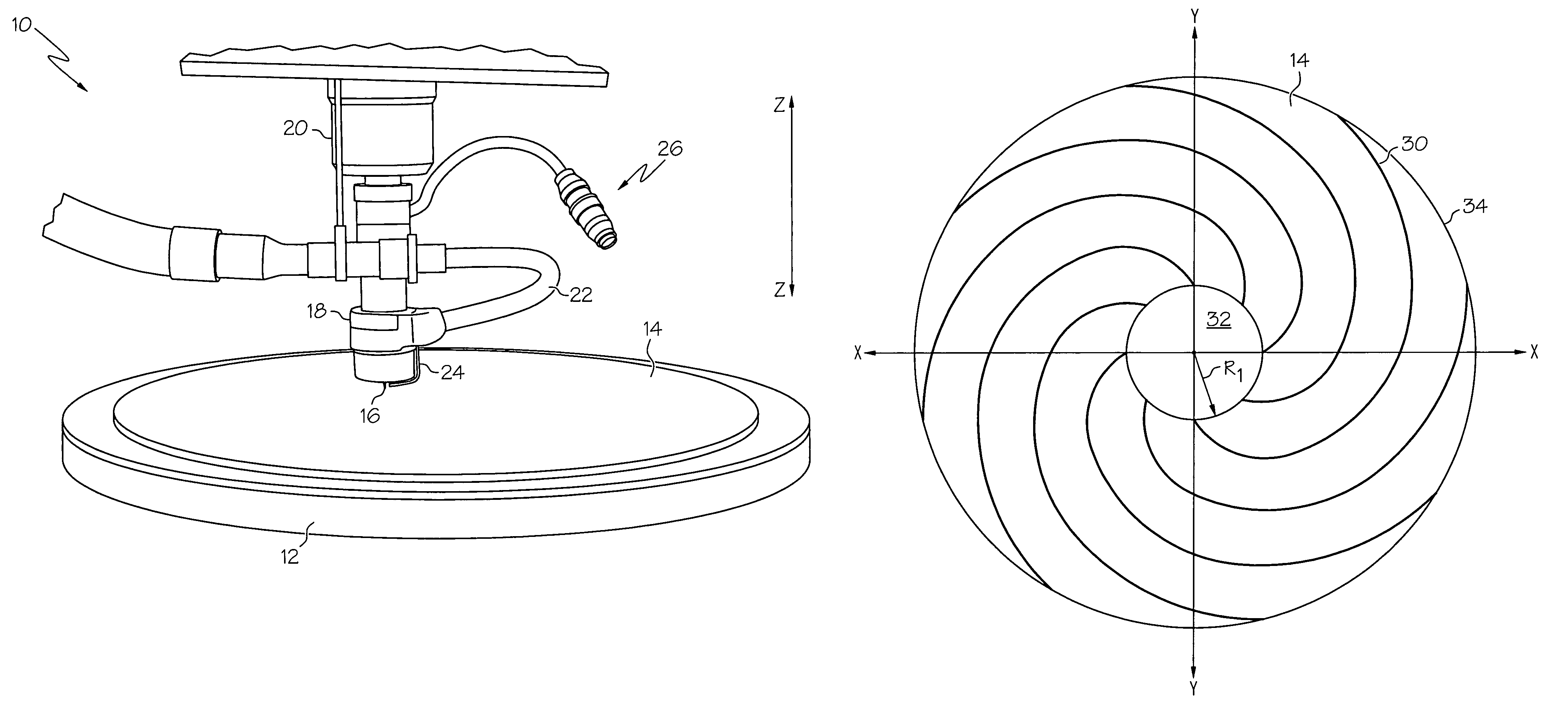
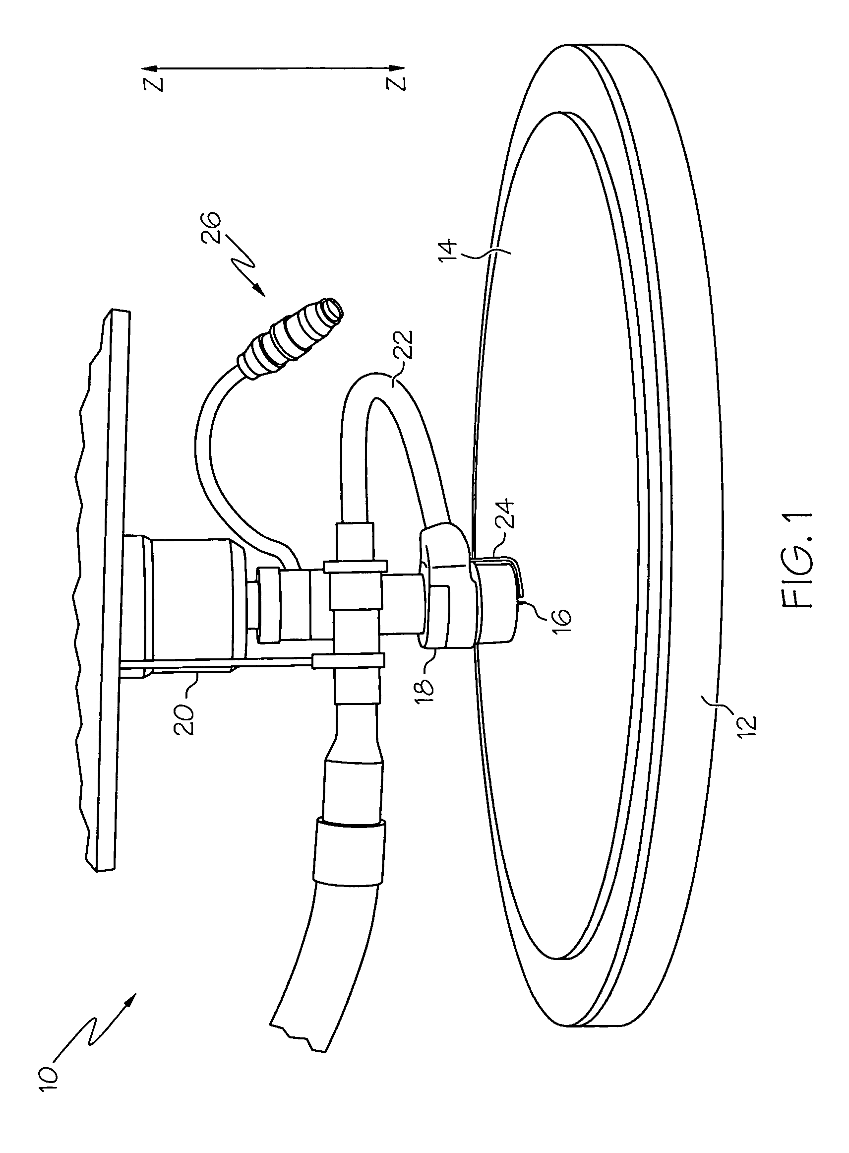
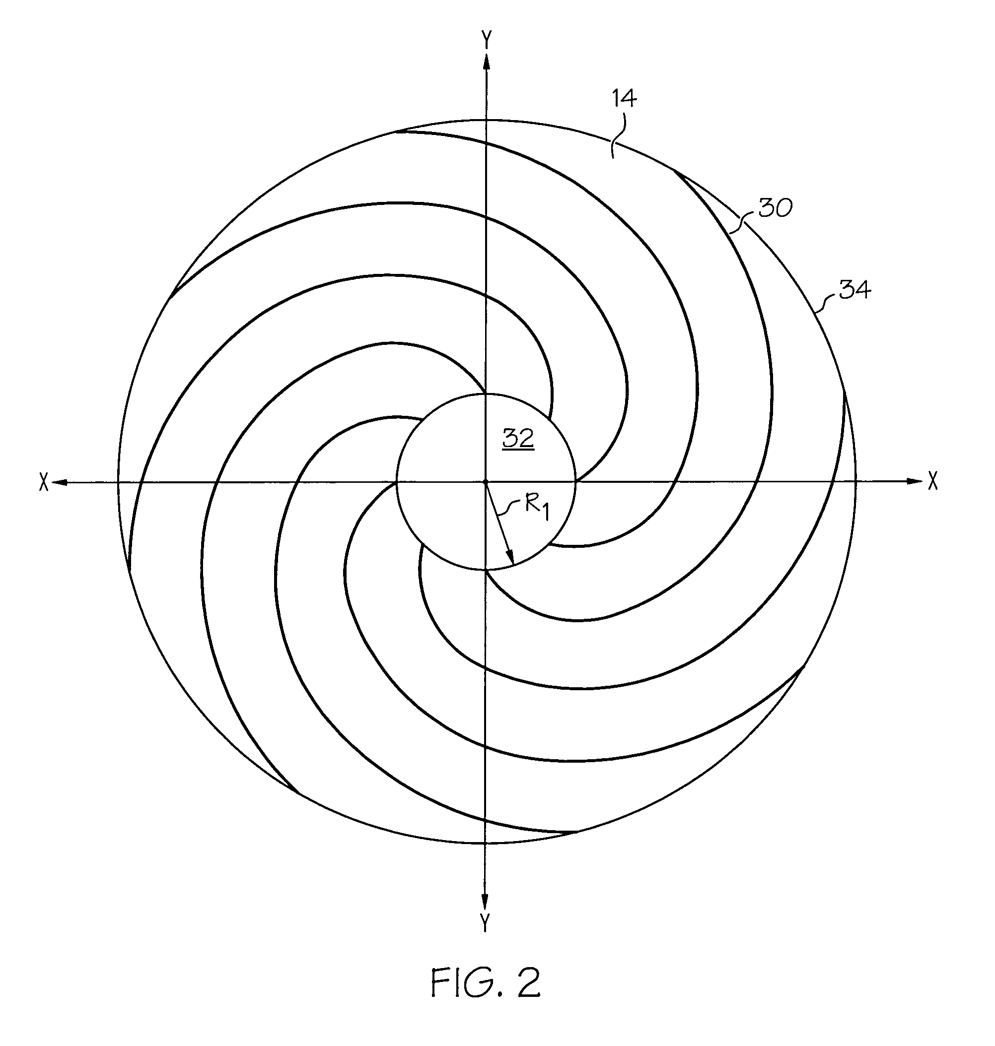
Curved grooving of polishing pads
a polishing pad and groove technology, applied in the field of polishing pads, can solve the problems of time-consuming and inefficient manufacturing process, the inability to produce only one groove at a time, and the inability to create grooves on the surface of cnc machines, and achieve the effect of a greater rate of production of grooves
- Summary
- Abstract
- Description
- Claims
- Application Information
AI Technical Summary
Benefits of technology
Problems solved by technology
Method used
Image

Examples
example 1
[0045]For harder materials like the IC1000™ polyurethane polishing pad, higher chip loading (for example, 0.0064 cm / rev.) produced better groove quality. Optimum operation was around 686 cm / min. (270 ipm) feed rate; and a 120 k rpm spindle speed produced the best groove quality on IC1000™ pads with either the PMT or KT tool bits.
Feed rate(ipm)=Chip load×Spindle speed(rpm)
example 2
[0046]For softer materials like VisionPad™ polyurethane polishing pads, lower chip loading (for example, 0.0044 cm / rev.) produced better groove quality. Optimum operation was around 533 cm / min. (210 ipm) feed rate and a 150 k rpm spindle speed produced the best groove quality on VisionPad™ polyurethane polishing pads with PMT tool bits.
[0047]
APPENDIX 1TableTopFeedSpindleChipGroovePadRateSpeedLoadBitQuality*Studymaterials(cm / min.)(RPM)(cm / rev.)Type(Grade A–D)Comment#1IC366 83 k0.0044PMTBBurrs atintersections, needair blast to clean outIC533120 k0.0044PMTBBurrs atintersections, needair blast to clean outIC762172 k0.0044PMTB−Lost of burrs atintersections, needair blast to clean outIC366 83 k0.0044PMTAIC533120 k0.0044PMTAIC762172 k0.0044PMTB+Both ends of groovelines not sharpIC366 83 k0.0044PMTAIC533120 k0.0044PMTAIC762172 k0.0044PMTB+Both ends of groovelines not sharpIC366 83 k0.0044PMTAIC533120 k0.0044PMTAIC762172 k0.0044PMTB+Groove edges notclean or sharp#2IC533120 k0.0044PMTAIC53312...
PUM
| Property | Measurement | Unit |
|---|---|---|
| Fraction | aaaaa | aaaaa |
| Speed | aaaaa | aaaaa |
| Speed | aaaaa | aaaaa |
Abstract
Description
Claims
Application Information