Semiconductor memory device with data bus scheme for reducing high frequency noise

Inactive Publication Date: 2007-07-03
SAMSUNG ELECTRONICS CO LTD
View PDF12 Cites 3 Cited by
  • Summary
  • Abstract
  • Description
  • Claims
  • Application Information

AI Technical Summary

Problems solved by technology

As a result, the difference between the operation speeds of the CPUs and memory devices continues to increase such that the operation speed of the memory devices becomes a major factor limiting the performance of a computer system.
However, since in line with the increasing operation speed, high frequency noise occurring in a computer system continues to increase, it is increasingly difficult to secure a voltage margin needed in system operation.
However, by the stub structure, discontinuity and impedance mismatching on the channel occur causing r

Method used


Image

  • Semiconductor memory device with data bus scheme for reducing high frequency noise
  • Semiconductor memory device with data bus scheme for reducing high frequency noise
  • Semiconductor memory device with data bus scheme for reducing high frequency noise

Examples


Embodiment Construction

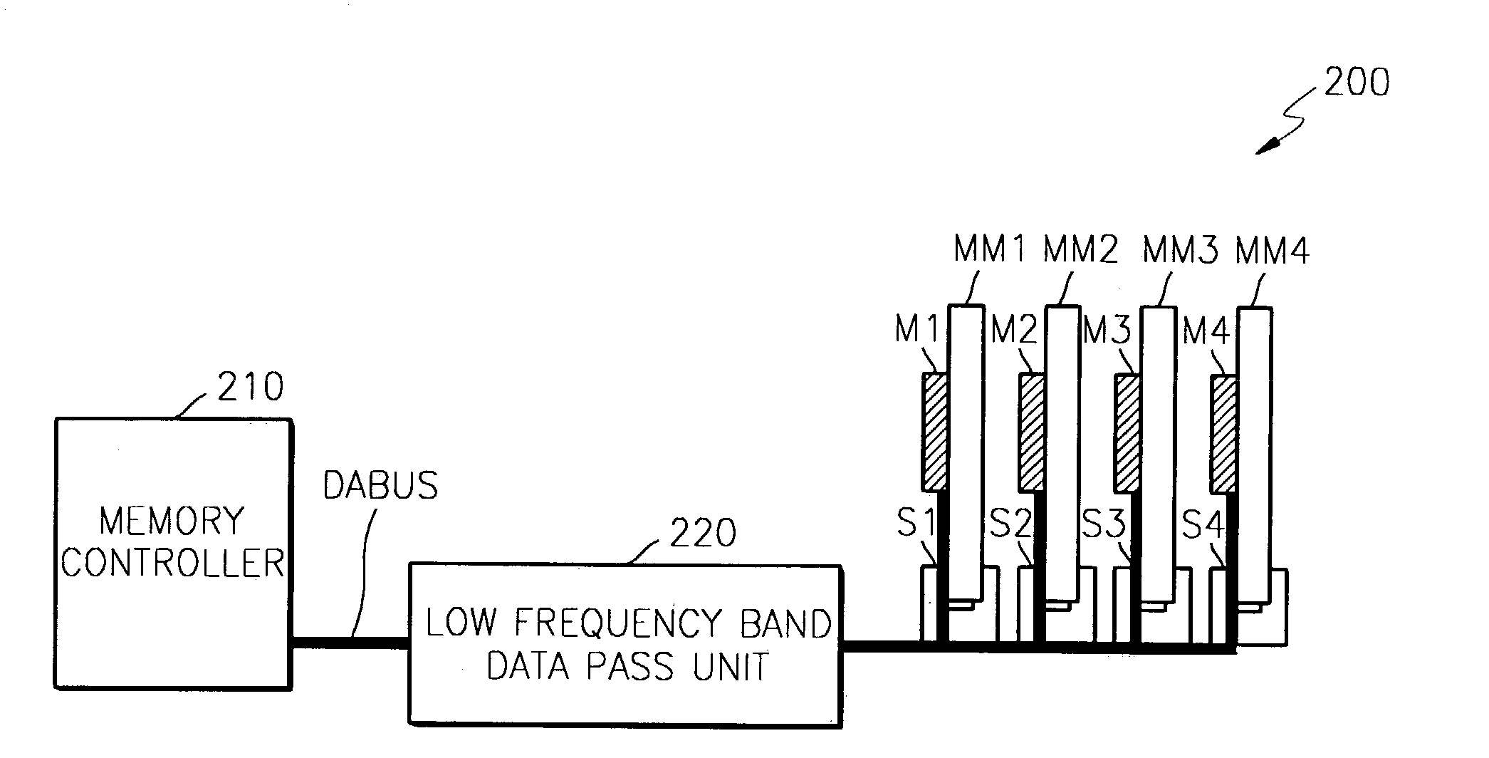
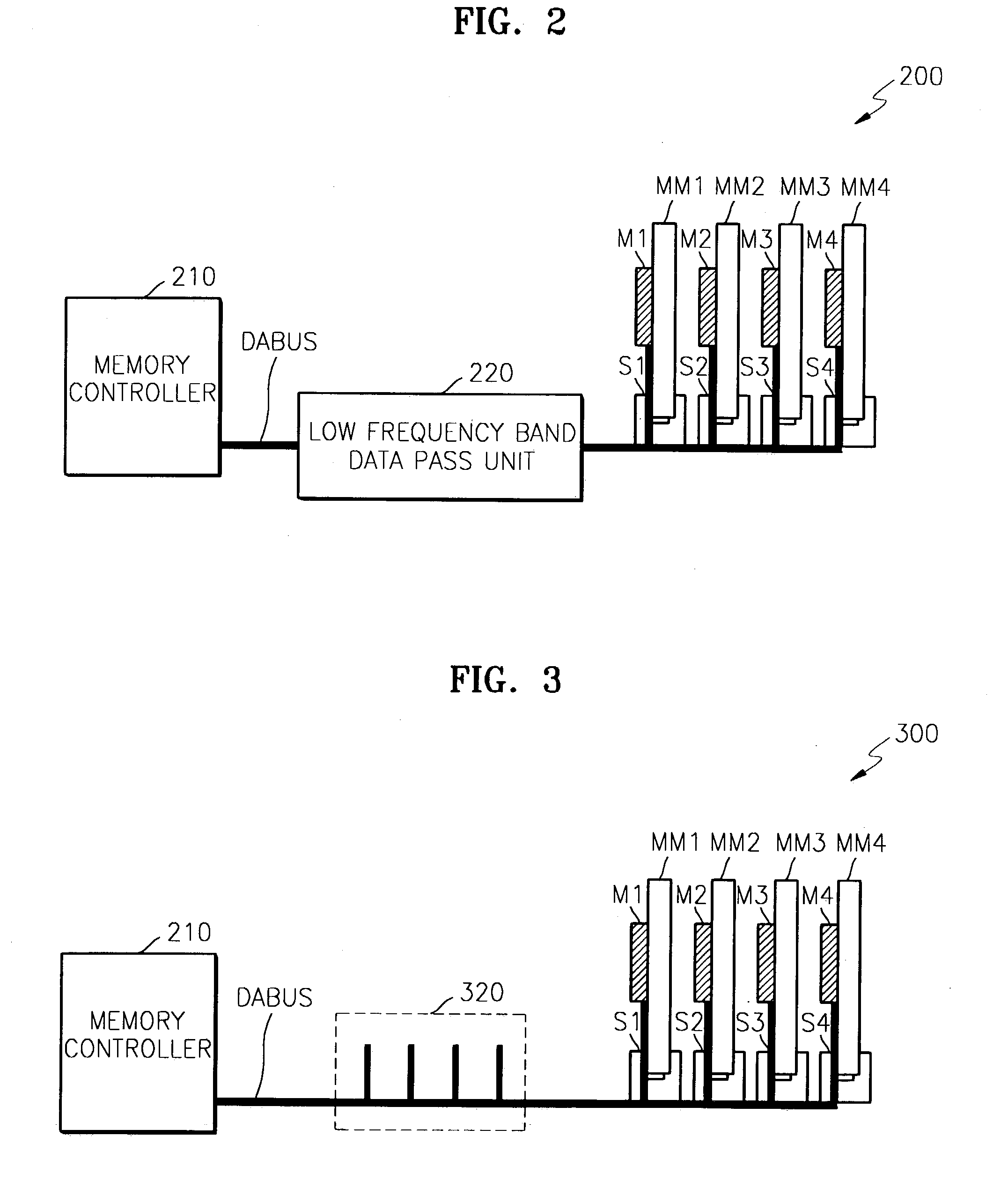
[0039]FIG. 2 is a schematic diagram showing a semiconductor memory device according to a first preferred embodiment.

[0040]Referring to FIG. 2, the semiconductor memory device 200 according to the first preferred embodiment comprises a plurality of memory modules MM1 through MM4, having respective memories M1 through M4, and a data bus (DABUS) which transfers data to the memory modules MM1 through MM4. The data bus (DABUS) includes a low frequency band data pass unit 220 which removes the high frequency component of data above a certain “cut-off” frequency, and transfers the filtered data to the memory modules MM1 through MM4.

[0041]The operation of the semiconductor memory device according to the first preferred embodiment will now be explained in detail referring to FIG. 2.

[0042]FIG. 2 shows the memory controller 210 which controls the memories M1 through M4, the memory modules MM1 through MM4, having respective memories M1 through M4, and slots S1 through S4 to which the memory mod...


PUM


Abstract

A semiconductor memory device includes memory modules which have memories and a data bus which transfers data to the memory modules, in which the data bus comprises a low frequency band data pass unit which removes the high frequency component of the data and sends the data to the memory modules. The low frequency band data pass unit comprises a plurality of stubs which are connected to the data bus in parallel and are formed as printed circuit board (PCB) patterns. The low frequency band data pass unit comprises a plurality of plates that are connected to the data bus in parallel and are formed as PCB patterns. The low frequency band data pass unit has a shape in which parts having a wide width and parts having a narrow width are alternately connected. Therefore, without adding a separate passive device, the semiconductor memory device reduces the high frequency noise of data transferred through a data bus such that the voltage margin of the data improves, the cost for passive devices such as capacitors, is reduced, and the process for attaching the passive devices is simplified.

Description

CROSS REFERENCES TO RELATED APPLICATIONS[0001]This application claims priority under 35 U.S.C. §119 from Korean Patent Application No. 2002-31410, filed on Jun. 4, 2002, the contents of which are hereby incorporated by reference in their entirety for all purposes as if fully set forth herein.BACKGROUND AND SUMMARY[0002]1. Technical Field[0003]The present invention relates to a semiconductor memory device, and more particularly, to a semiconductor memory device having a data bus structure which reduces high frequency noise to data and passes only data having a low frequency.[0004]2. Description of the Related Art[0005]Semiconductor memory devices have been developed focusing on high integration and high capacity based on the high integration, while central processing units (CPUs) that are cores of computer system have been developed mainly focusing on high speed operation.[0006]As a result, the difference between the operation speeds of the CPUs and memory devices continues to increa...

Claims


Application Information

Patent Timeline
IPC IPC(8): H01P5/12G06F13/16G06F12/00G06F13/00G06F13/40G11C7/10
CPCG11C7/1006H05K1/0216H05K1/14H05K2201/044H05K2201/09727H05K2201/09781H05K1/0237G06F13/40
Inventor PARK, MYUN-JOOLEE, JAE-JUN
Owner SAMSUNG ELECTRONICS CO LTD
Why Eureka
Try Eureka