Method for manufacturing semiconductor device having trench in silicon carbide semiconductor substrate

a semiconductor substrate and manufacturing method technology, applied in semiconductor devices, single crystal growth, chemistry apparatus and processes, etc., can solve the problems of inability to solve conventional techniques, the thickness of unnecessary epitaxial film removed in the etch-back step after the embedding step may surely exceed the depth of the trench, etc., to achieve uniform impurity concentration profile, excellent on-off performance, and uniform shape

Active Publication Date: 2007-07-10
DENSO CORP
View PDF25 Cites 37 Cited by
  • Summary
  • Abstract
  • Description
  • Claims
  • Application Information

AI Technical Summary

Benefits of technology

[0016]In view of the above-described problem, it is an object of the present invention to provide a method of manufacturing a semiconductor device having a trench in a silicon carbide semiconductor substrate. The device has excellent crystallinity.

Problems solved by technology

However, in the case that the N type channel layer and the P+ type gate region, which will be formed inside the trench in the silicon carbide trench J-FET disclosed in JP-A-2003-69041, such a problem occurs which cannot be solved by the above-explained conventional techniques.
More specifically, in such a case that the aspect ratio of the trench is equal to or larger than 2, and the inclination angle is substantially vertical, this problem may occur which cannot be solved by the conventional techniques.
In addition, since the growth rate of the trench inner portion is necessarily lower than that of the non-trench portion, even when the P+ type gate region could be embedded without an occurrence of such a cavity, there is another problem that the removing film thickness of the unnecessary epitaxial film in the etch-back step after the embedding step may surely become larger than the depth of the trench.
However, the above documents do not clarify a difference between the growth rates depending upon the face orientation.
Furthermore, the above documents never disclose any clear indications how to increase the growth rate of the trench inner portion, as compared with that of the non-trench portion, and also how to decrease the removing film thickness of the unnecessary epitaxial film in the etch-back step after the embedding process.
However, there are other problems.
Also, a sacrifice oxidation owns such a problem that an oxidation rate is low and a long oxidation time is required.
However, the mechanism as to Si is completely different from the mechanism as to silicon carbide.
As a result, when the thermal process is carried out in the hydrogen atmosphere to which HCl is not added under the normal pressure, only C elements are removed, and removing of Si elements is disturbed.
Therefore, there are various problems: a difference in etching rates depending upon face orientation of etching planes is not clarified; how to round a trench corner portion while preventing the surface reaction rate controlling by which a plurality of facet planes are produced; and also, the condition thereof is not clarified.
Furthermore, in the case that the trench etching damage region of the trench inner planes (side plane and bottom plane) has been removed, there is no clear indication as to the reducing effects for reducing the surface convexs / concaves, and the crystal defects.

Method used


Image

  • Method for manufacturing semiconductor device having trench in silicon carbide semiconductor substrate
  • Method for manufacturing semiconductor device having trench in silicon carbide semiconductor substrate
  • Method for manufacturing semiconductor device having trench in silicon carbide semiconductor substrate

Examples


first embodiment

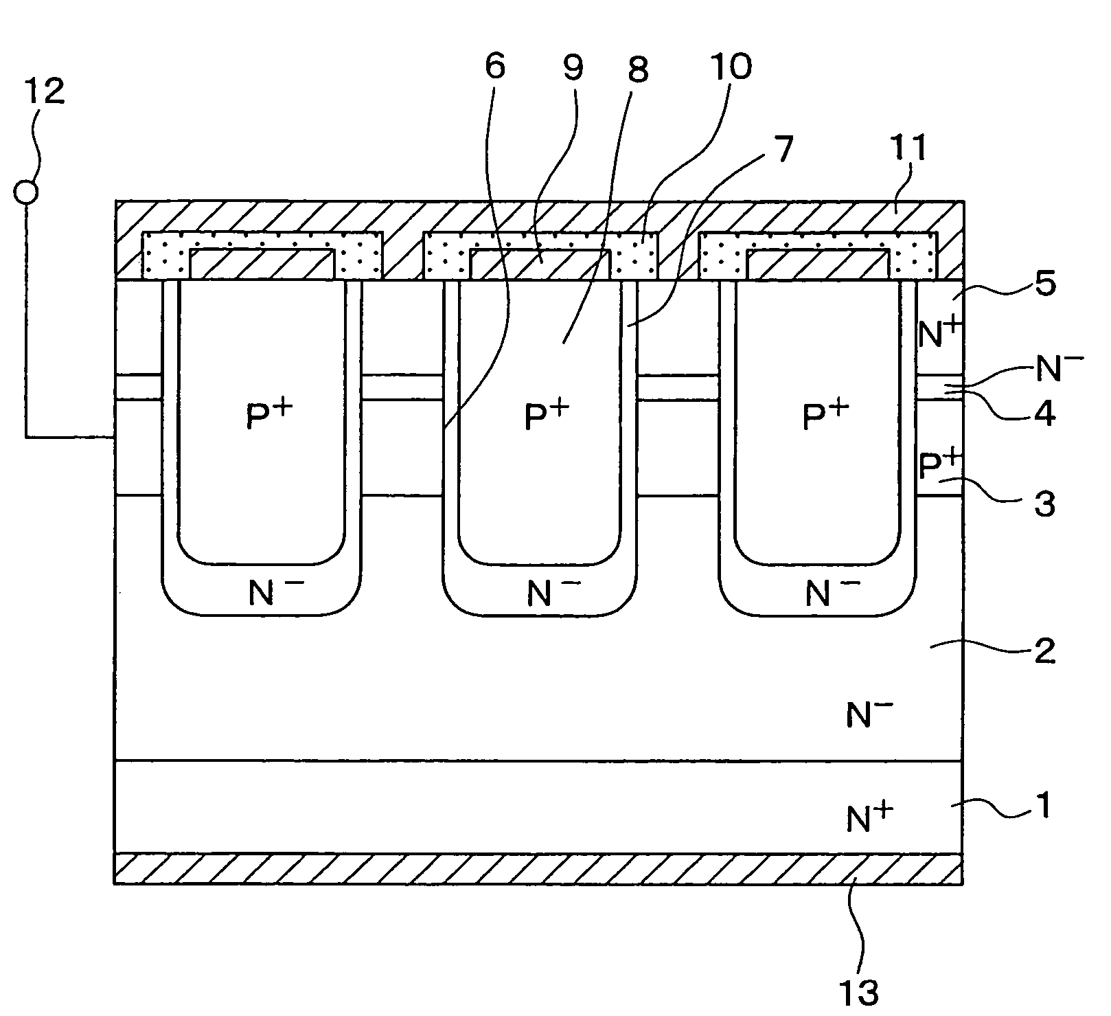
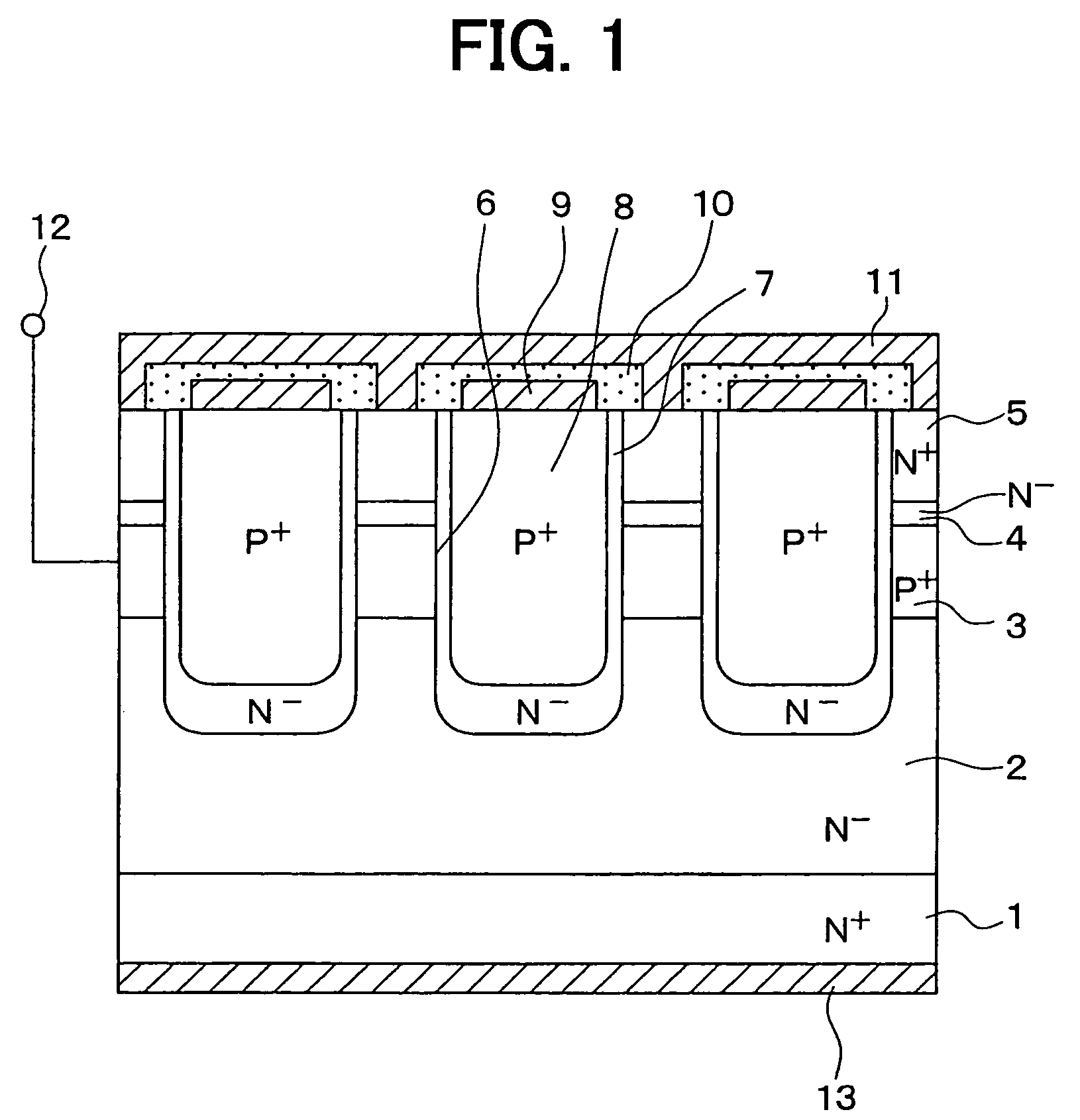
[0116]FIG. 1 shows a sectional structure of a J-FET provided in a silicon carbide semiconductor device according to a first embodiment of the present invention. The structure of the J-FET will now be described with reference to FIG. 1.

[0117]As indicated in FIG. 1, while an N+ type substrate 1 having a silicon carbide “(0001) Si” face has been employed and this N+ type substrate 1 is made in high impurity concentration equal to or higher than, for instance, 1×1019 cm−3, an N− type drift layer 2 has been formed on a major surface of this N+ type substrate 1, and this N− type drift layer 2 is made in low impurity concentration of, for example, 1×10¹³ to 5×1015 cm−3. Also, a first gate region 3 made of a P+ type layer has been epitaxial-grown on the surface of the N− type drift layer 2. This first gate region 3 is made in high impurity concentration of, for example, 5×10¹⁷ to 5×1019 cm−3.

[0118]Further, an N− type region 4 has been epitaxial-grown on the surface of the first gate region ...

second embodiment

[0156]Next, a description is made of a semiconductor device manufacturing method according to a second embodiment mode of the present invention. Since this second embodiment mode is substantially same as the first embodiment mode, different points from those of the first embodiment mode will now be mainly explained.

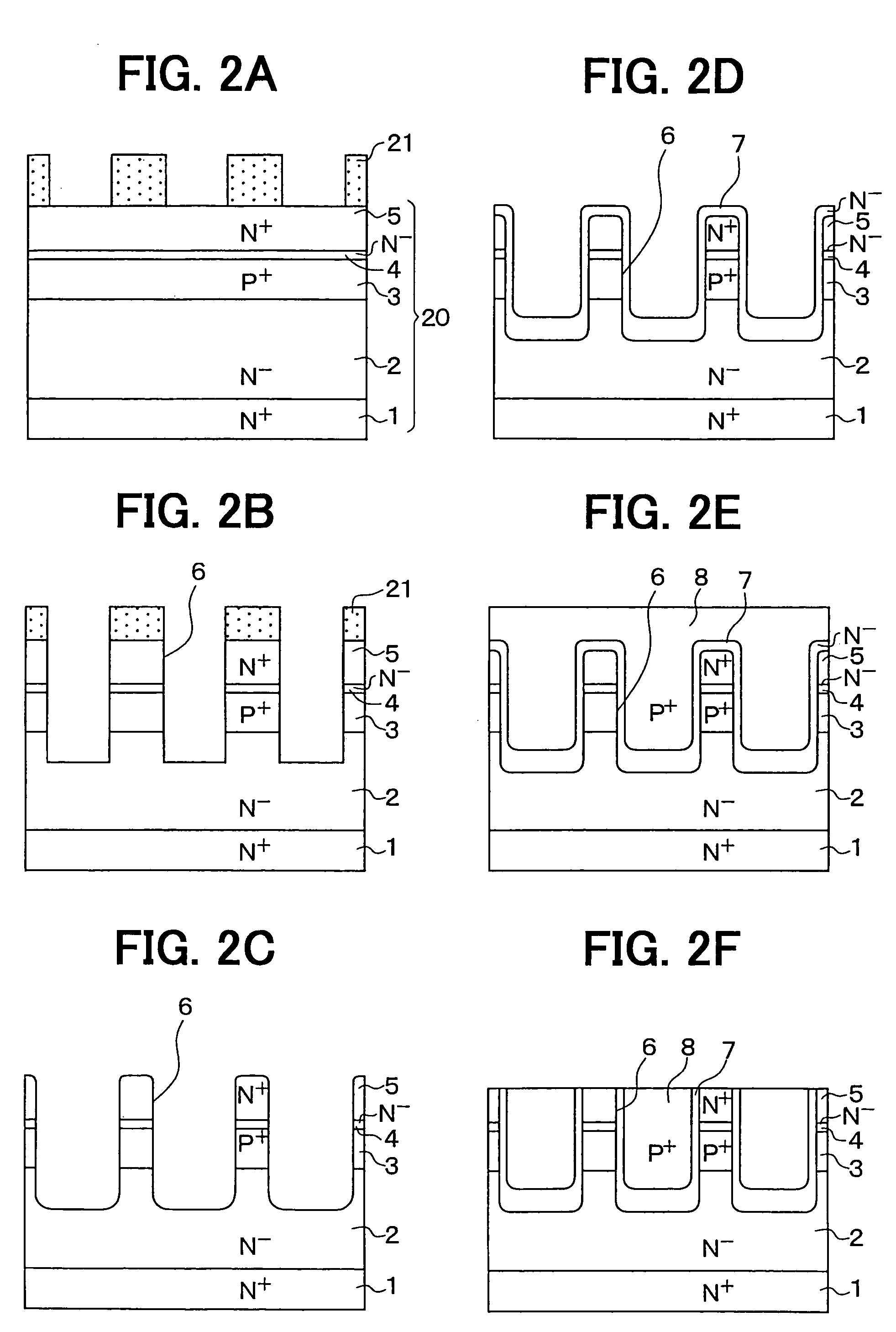
[0157]FIGS. 4A to FIG. 4E are sectional views for schematically showing steps for manufacturing a semiconductor device according to a second embodiment of the present invention. These sectional views indicate steps for manufacturing an N− type channel layer 7 and a P+ type of a second gate region 8 of a trench type J-FET similar to the first embodiment mode. In this second embodiment mode, a selective epitaxial-purpose mask is not formed in a trench 6 of a transistor cell portion, but is applied only to a trench of an alignment key region. As a result, an alignment of an embedding epitaxial step and alignments of an etch-back step and succeeding steps is secured.

[0158]Fir...

third embodiment

[0166]Next, a description is made of a semiconductor device manufacturing method according to a third embodiment mode of the present invention. Since this third embodiment mode is substantially same as the first embodiment mode, different points from those of the first embodiment mode will now be mainly explained.

[0167]A third embodiment of the present invention is realized by executing the first embodiment mode, and by changing only a growth condition in an epitaxial step. That is, while such an etching gas as hydrogen chloride is mixed with SiH4 and C3H8 corresponding to the material gas, and H2 corresponding to the carrier gas, an epitaxial growing process is carried out. Concretely speaking, although depending upon a substrate temperature, while hydrogen chloride gas in approximately 1 to 5% of a hydrogen gas flow rate is mixed with the material gas and the carrier gas, the epitaxial growing process is carried out.

[0168]Since such a gas having the etching effect is conducted, ev...


PUM

PropertyMeasurementUnit
trench slanting angleaaaaaaaaaa
aspect ratioaaaaaaaaaa
temperatureaaaaaaaaaa

Abstract

A method for manufacturing a silicon carbide semiconductor device includes the steps of: forming a trench mask on an upper surface of a semiconductor substrate; forming the trench such that the trench having an aspect ratio equal to or larger than 2 and having a trench slanting angle equal to or larger than 80 degrees is formed; and removing a damage portion in such a manner that the damage portion disposed on an inner surface of the trench formed in the semiconductor substrate in the step of forming the trench is etched and removed in hydrogen atmosphere under decompression pressure at a temperature equal to or higher than 1600° C.

Description

CROSS REFERENCE TO RELATED APPLICATIONS[0001]This application is based on Japanese Patent Applications No. 2004-118890 filed on Apr. 14, 2004, No. 2004-193459 filed on Jun. 30, 2004, and No. 2004-193460 filed on Jun. 30, 2004, the disclosures of which are incorporated herein by reference.FIELD OF THE INVENTION[0002]The present invention relates to a method for manufacturing a semiconductor device having a trench in a silicon carbide semiconductor substrate.BACKGROUND OF THE INVENTION[0003]Conventionally, the embedding technique of the silicon carbide semiconductors is disclosed in, for example, Materials Science Forum P131–134, Vols. 264–268, 1988.[0004]In this document, while various samples were employed, the trench inclination angles of which are approximately 50 degrees, and these samples own various sorts of trench widths, the aspect ratios of which are equal to or smaller than 1, such experiments have been carried out. That is, the epitaxial growing processes have been perform...

Claims


Application Information

Patent Timeline
Patent Type & Authority Patents(United States)
IPC IPC(8): H01L21/18H01L21/302H01L21/308C30B23/02H01L21/04H01L21/306H01L21/337H01L21/76H01L29/04H01L29/24H01L29/78H01L29/808
CPCH01L29/045H01L29/66068H01L29/7828H01L29/8083
Inventor TAKEUCHI, YUUICHIMALHAN, RAJESH KUMARMATSUNAMI, HIROYUKIKIMOTO, TSUNENOBU
Owner DENSO CORP
Why Eureka
Try Eureka