
Method of manufacturing a semiconductor memory device including a transistor

a semiconductor memory and transistor technology, applied in semiconductor devices, capacitors, electrical devices, etc., can solve the problems of difficult to overcome a short channel effect, difficult to maintain a stable and steady operation of the memory device, and increase the electrical resistance of the contact plug, so as to minimize the electrical resistance of the contact pad, improve the operation characteristic of the dram device, and reduce the leakage current of the junction

Inactive Publication Date: 2007-07-24
SAMSUNG ELECTRONICS CO LTD
View PDF11 Cites 12 Cited by
  • Summary
  • Abstract
  • Description
  • Claims
  • Application Information

AI Technical Summary

Benefits of technology

The present invention provides a semiconductor device with reduced junction leakage current and electrical resistance of the contact at source / drain regions. This is achieved by forming a channel doping region in the substrate between predetermined adjacent gate structures, which includes a first impurity region surrounded by a second impurity region. The method of manufacturing the semiconductor device includes forming a plurality of gate structures on a substrate, forming a gate spacer on the sidewall of each gate structure, and forming a semiconductor pattern on the substrate between the gate structures. The semiconductor pattern includes a first impurity region and a second impurity region at surface portions of the substrate. The first and second impurity regions are formed by implanting a first conductive type impurity and a second conductive type impurity, respectively. The method also includes forming a first insulation interlayer on the substrate including the plurality of gate structures, forming first and second contact pads through the first insulation interlayer, and forming a contact hole in the second insulation interlayer for exposing the first contact pad. The semiconductor device and method of manufacturing the same provide improved performance and reliability.

Problems solved by technology

Thus, it is difficult to maintain a stable and steady operation in the memory device, which is important when a design rule of the memory device is smaller than about 0.1 μm.
For example, it becomes difficult to overcome a short channel effect as a gate length of a memory device is shortened.
Thus, an electrical resistance of the contact plug is increased and becomes an obstacle to the stable and steady operation of the memory device.
However, the recessed transistor has a problem in that an operation characteristic of a left portion of the transistor is different from that of a right portion of the transistor when the gate trench on the substrate is not aligned to a gate electrode pattern.
The recessed transistor also has a problem in that a parasite capacitance of a word line is increased in a memory device since a surface of a gate oxide layer is increased as compared with a conventional planar transistor.
The increased parasite capacitance reduces an operation speed of the recessed transistor.

Method used


Image

  • Method of manufacturing a semiconductor memory device including a transistor
  • Method of manufacturing a semiconductor memory device including a transistor
  • Method of manufacturing a semiconductor memory device including a transistor

Examples


Embodiment Construction

[0024]Preferred embodiments of the present invention will be described below in more detail with reference to the accompanying drawings. The present invention may, however, be embodied in different forms and should not be construed as limited to the embodiments set forth herein. Rather, these embodiments are provided so that this disclosure will be thorough and complete, and will fully convey the scope of the present invention to those skilled in the art.

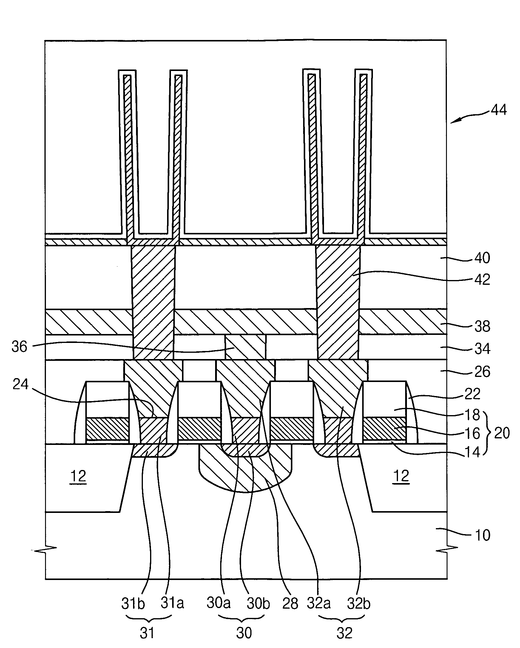
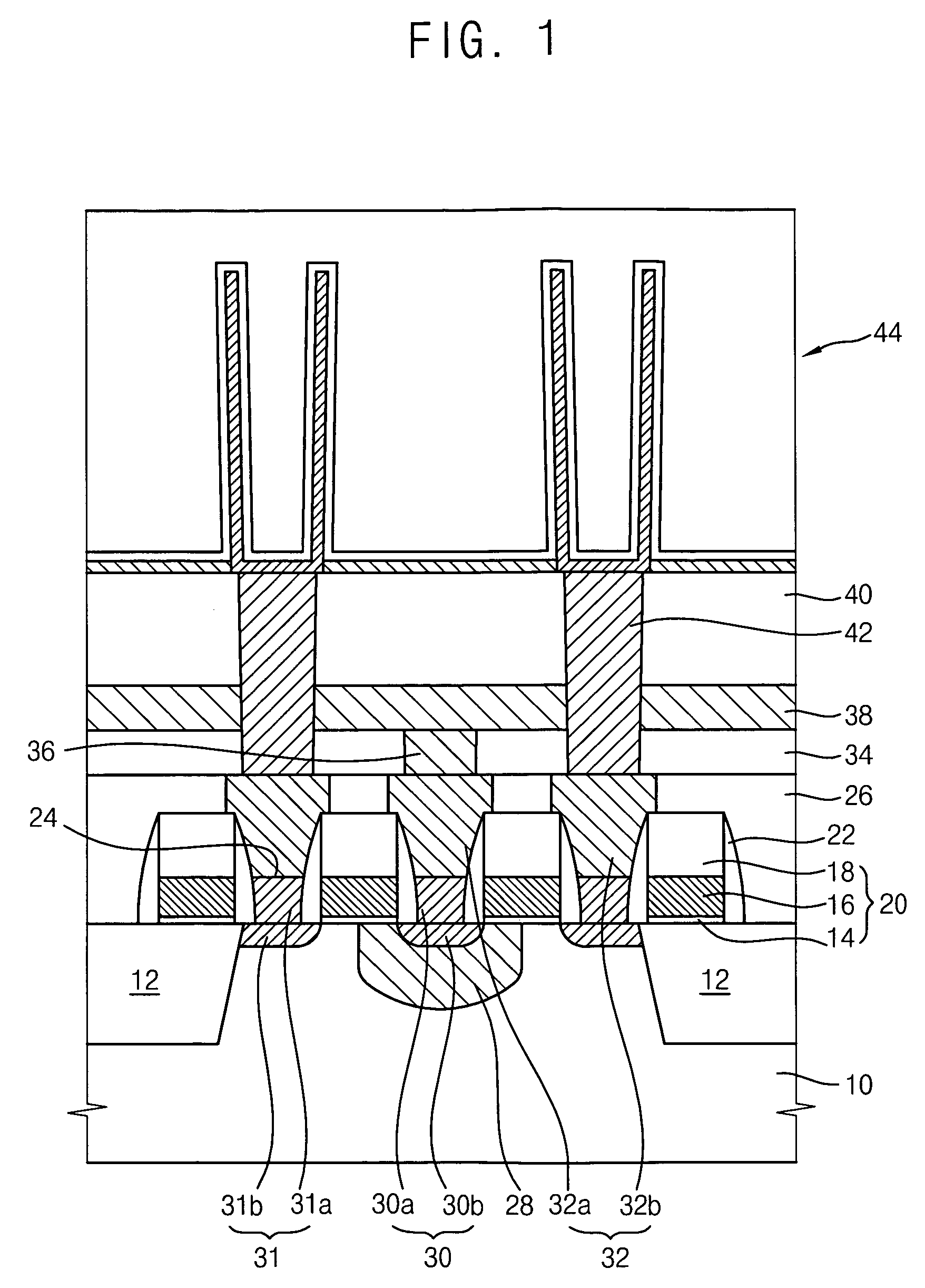
[0025]FIG. 1 is a cross sectional view illustrating a DRAM device including a planar gate electrode according to an embodiment of the present invention.

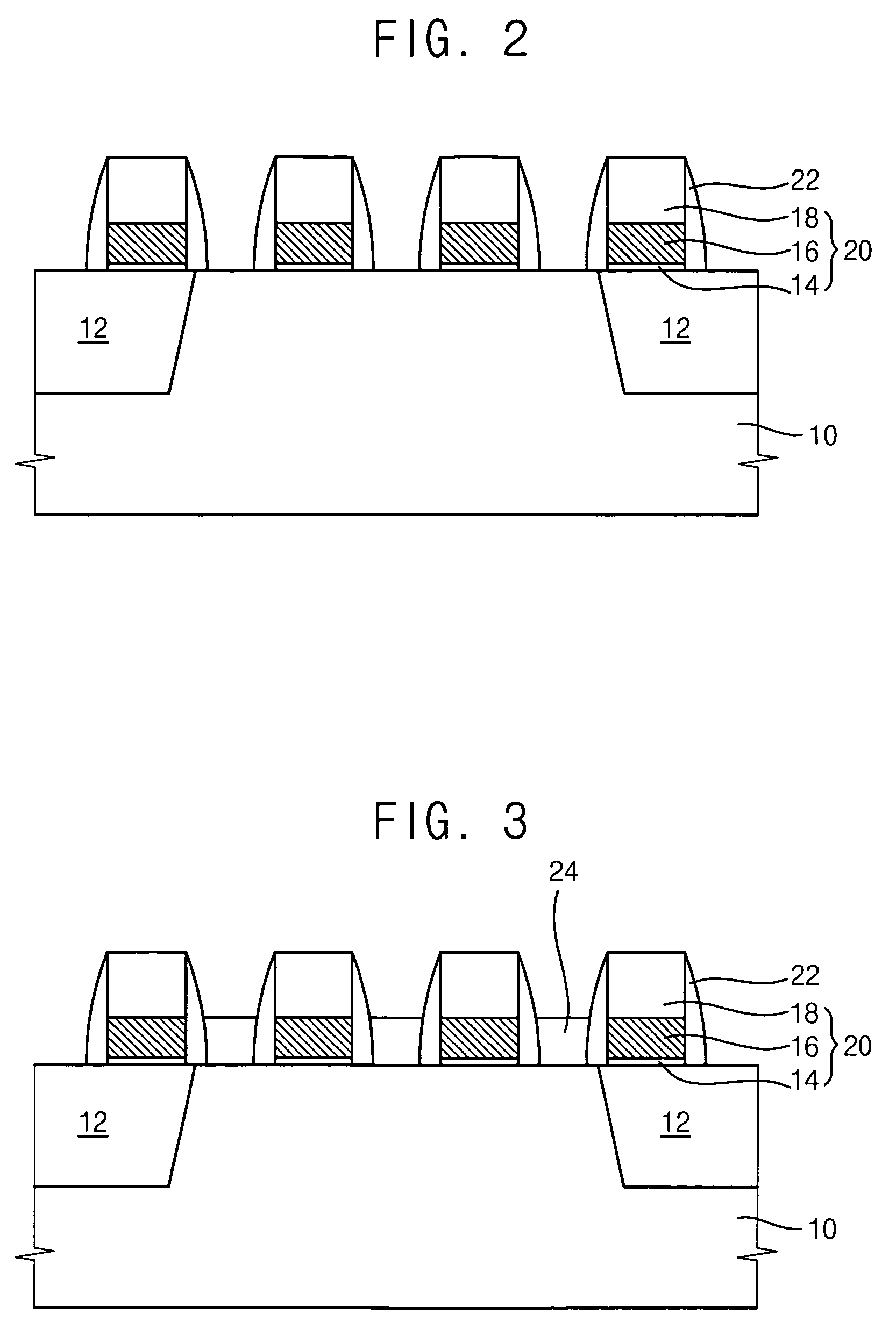
[0026]Referring to FIG. 1, a semiconductor substrate 10 such as a silicon wafer is separated into a field region 12 and an active region. A device isolation layer is formed in the field region 12 by a trench isolation process.

[0027]A gate structure 20 is formed on the active region of the substrate 10 as a linear pattern shape, and includes a gate insulation pattern 14, a gate conduc...


PUM


Abstract

A semiconductor device comprises a plurality of gate structures formed on a substrate, a gate spacer formed on a sidewall of the gate structures, a semiconductor pattern formed on the substrate between the gate structures, a first impurity region and a second impurity region formed in the semiconductor pattern and at surface portions of the substrate, respectively, wherein the first and second impurity regions include a first conductive type impurity, and a channel doping region surrounding the first impurity region, wherein the channel doping region includes a second conductive type impurity.

Description

CROSS-REFERENCE TO RELATED APPLICATION[0001]This application claims priority to Korean Patent Application No. 2004-52685 filed on Jul. 7, 2004, the content of which is herein incorporated by reference in its entirety.TECHNICAL FIELD[0002]The present disclosure relates to a semiconductor device and a method of manufacturing the same, and more particularly to a semiconductor memory device including a transistor and a method of manufacturing the same.DISCUSSION OF RELATED ART[0003]Integration degree, reliability and the response speed of semiconductor devices need to be improved to operate the semiconductor devices at a high speed and to have a large storing capacitance.[0004]A dynamic random access memory (DRAM) device is an example of the semiconductor device having characteristics of a large storing capacitance and a high facility of storing and erasing data. The DRAM device includes a memory cell for storing data using electric charges and peripheral circuits for transferring the e...

Claims


Application Information

Patent Timeline
Patent Type & Authority Patents(United States)
IPC IPC(8): H01L21/336H01L21/02H10B12/00
CPCH01L27/10814H01L27/10823H01L27/10876H01L27/10885H01L27/10888H01L29/6659H01L27/10852H01L27/10873H01L28/91H10B12/34H10B12/315H10B12/033H10B12/05H10B12/053H10B12/482H10B12/485H01L21/18H10B99/00H10B12/00
Inventor LEE, JIN-WOOYUN, CHEOL-JUSEO, HYEOUNG-WON
Owner SAMSUNG ELECTRONICS CO LTD
Learn More