MOSFET formed on a silicon-on-insulator substrate having a SOI layer and method of manufacturing

a silicon-on-insulator and substrate technology, applied in the direction of semiconductor devices, semiconductor/solid-state device details, electrical apparatus, etc., can solve the problems of aggregation of silicide, easy deterioration of transistors of the full depletion type, and difficult circuit design

Inactive Publication Date: 2007-07-24
NEC CORP
View PDF16 Cites 11 Cited by
  • Summary
  • Abstract
  • Description
  • Claims
  • Application Information

AI Technical Summary

Problems solved by technology

This makes a circuit design difficult.
However, transistors of the full depletion type are subject to a characteristic deterioration caused by a punch through and a short channel effect, compared to transistors of the partially depleted type.
In particular, if a metal silicide layer is formed on the source / drain region, the whole film thickness of the silicon layer is silicified, which causes a problem that an aggregation of silicide and breaking of wire may easily occur, whereby the parasitic resistance increases.
As such, it is difficult to form elevated layers with low resistance.
Further, the selective epitaxial growth needs a special CVD device suitable for the method, which causes the manufacturing cost to increase.
In this case, however, the surface height of the gate electrode and the surface height of the elevated layer coincide with each other, which causes a problem that a short circuit tends to occur when a silicide layer is formed.

Method used


Image

  • MOSFET formed on a silicon-on-insulator substrate having a SOI layer and method of manufacturing
  • MOSFET formed on a silicon-on-insulator substrate having a SOI layer and method of manufacturing
  • MOSFET formed on a silicon-on-insulator substrate having a SOI layer and method of manufacturing

Examples


first embodiment

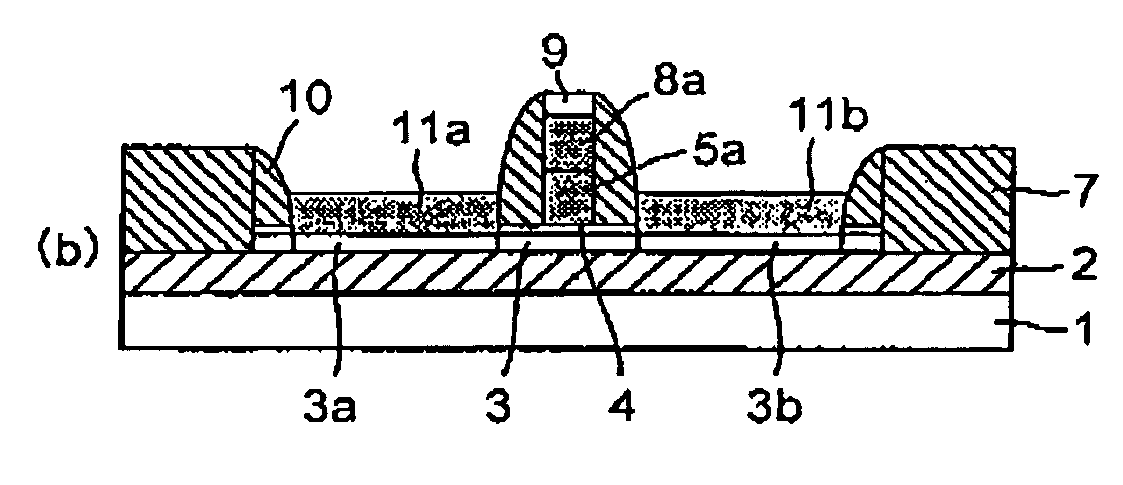
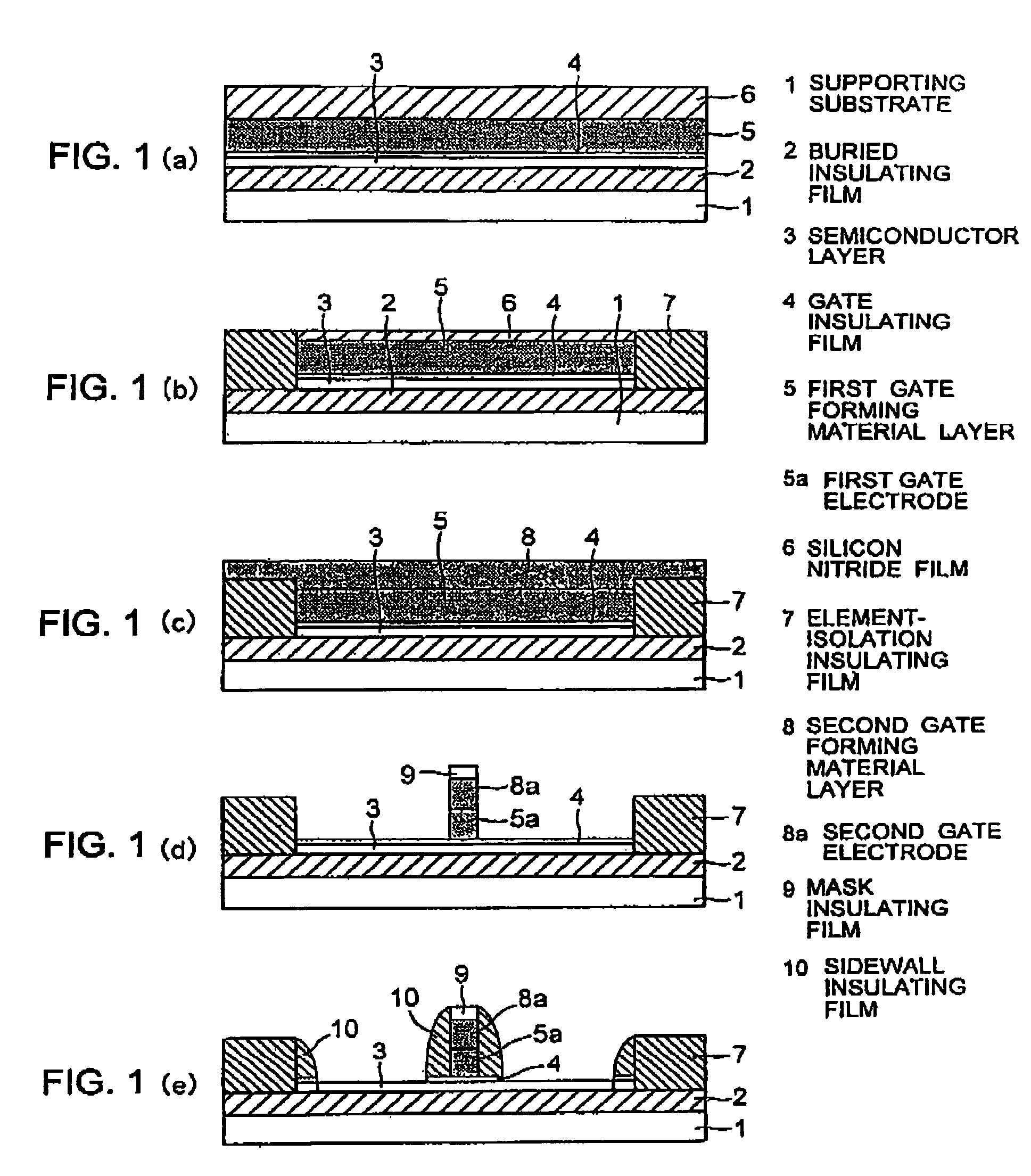
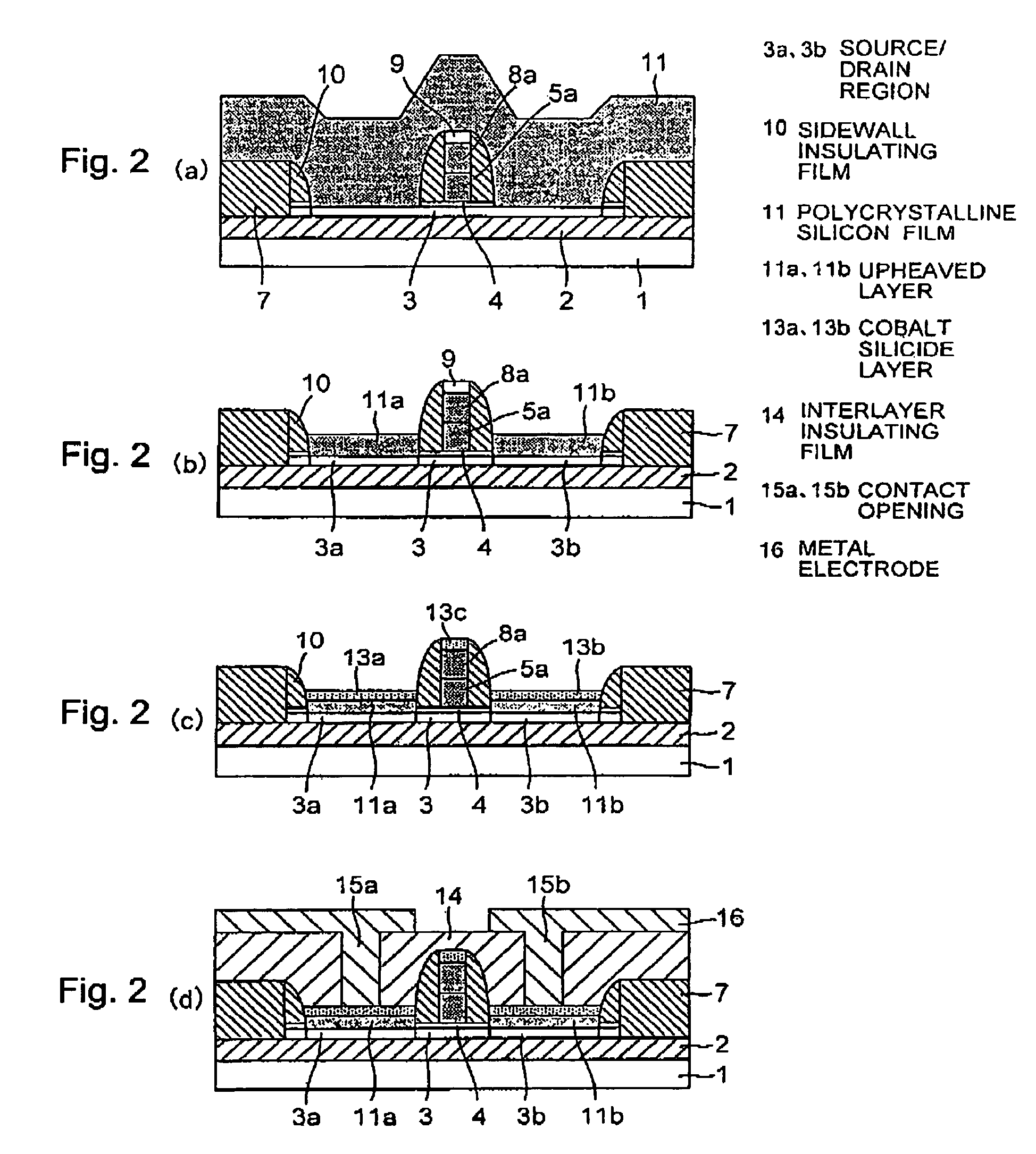
[0039]FIGS. 1(a) through 1(e) and FIGS. 2(a) through 2(d) are schematic sectional views showing the steps of a manufacturing method of a semiconductor device, in order, according to a first embodiment of the present invention. In FIGS. 1 and 2, the dimensions in the vertical direction (up and down direction of the Figs.) are shown to be enlarged.

[0040]As shown in FIG. 1(a), first there is provided an SOI substrate in which, on a supporting substrate 1 made of silicon or the like, a buried insulating film 2 consisting of an oxide film with a thickness of 100 nm is formed, then on the insulating film 2, a semiconductor layer 3 made of silicon or the like is formed to have a film thickness of 5 nm to 60 nm. As a substitute for such an SOI substrate, an SOI substrate formed by an SIMOX (Separated by Implanted Oxygen) method in which oxygen is ion-implanted into a silicon supporting substrate, or an SOI substrate formed by laminating, may be used. Further, an SOI substrate in which a sem...

second embodiment

[0059]FIG. 4 is a sectional view showing a second embodiment of the present invention. In FIG. 4, the dimension in the vertical direction (up and down direction in the Fig.) is shown to be enlarged.

[0060]A semiconductor device according to the second embodiment shown in FIG. 4 includes, a buried insulating film 2 formed on a supporting substrate 1, a semiconductor layer 3 consisting of a silicon film, source / drain regions 3a, 3b formed in a portion thereof, element-isolation insulating films 7 surrounding the semiconductor layer 3, a gate insulating film 4 formed on the semiconductor layer 3, a first gate electrode 5a and a second gate electrode 8a, sidewall insulating films 10 formed on the sidewalls of the gate electrodes, elevated layers 11c, 11d consisting of a metal silicide film formed to be buried in depressions surrounded by the element-isolation insulating films 7 (and the sidewall insulating films 10 thereof) and by the gate electrodes (and the sidewall insulating films 10...

third embodiment

[0066]FIGS. 5(a) through 5(e) and FIGS. 6(a) through 6(d) are schematic sectional views showing the manufacturing method in the order of steps of a semiconductor device according to a third embodiment of the present invention. In FIGS. 5 and 6, the dimensions in the vertical direction (up and down direction in Figs.) are shown to be enlarged.

[0067]First, as shown in FIG. 5(a), there is provided an SOI substrate which is so formed that on a supporting substrate 1 consisting of silicon or the like, a buried insulating film 2 consisting of, for example, an oxide film having a film thickness of 100 nm and a semiconductor layer 3 having a film thickness of 5 nm to 60 nm consisting of silicon or the like are laminated.

[0068]Next, impurity atoms of a first conductive type are implanted into the semiconductor layer by, for example, the ion implanting so as to be in a concentration appropriate for forming a channel region. Then, on the semiconductor layer 3, a gate oxide layer with about 10 ...


PUM


Abstract

In a FET having a thin-film SOI layer, to prevent a parasitic resistance increase in source / drain regions. To realize an elevated layer to be formed on the source / drain region without using a lithography process and without a fear of a short circuit. Element-isolation insulating films 7, which are taller than a semiconductor layer 3, are formed surrounding the island-shaped semiconductor layer (SOI layer) 3, while gate electrodes 5a, 8a which are taller than the element-isolation insulating films 7 are formed on the semiconductor layer 3. A polycrystalline silicon film 11 is deposited on the whole surface. elevated layers 11a, 11b which are shorter than the element-isolation insulating film 7 are formed on the source / drain regions 3a, 3b by chemical-mechanical polishing and etching back. Silicide layers 13a to 13c are formed on the gate electrode and on the elevated layers. An interlayer insulating film 14 is formed, and a metal electrode 16 is formed.

Description

TECHNICAL FIELD[0001]The present invention relates to a semiconductor device and its manufacturing method, and in particular, to a MOSFET formed on a silicon-on-insulator (hereinafter abbreviated as SOI) substrate having an SOI layer, and its manufacturing method.BACKGROUND ART[0002]In a case of forming a MOSFET using an SOI substrate in which a single crystal semiconductor layer (silicon layer) is formed on a semiconductor supporting substrate via an insulating film (mainly an oxide film), the insulating film is formed under the source region and the drain region of the MOSFET, whereby it is possible to reduce the parasitic capacity comparing to a case where a MOSFET is formed using a typical bulk substrate. As such, manufacturing an LSI with a use of an SOI substrate is advantageous for a speedup of the element, so that this method has been widely adopted.[0003]In general, MOSFETs using SOI substrates may be of a full depletion type in which an SOI layer below the gate is fully de...

Claims


Application Information

Patent Timeline
Patent Type & Authority Patents(United States)
IPC IPC(8): H01L27/01H01L21/28H01L21/285H01L21/336H01L21/60H01L29/423H01L29/45H01L29/786
CPCH01L21/28518H01L21/76897H01L29/41783H01L29/458H01L29/66772H01L29/78618H01L29/42384H01L2924/0002H01L2924/3011H01L2924/00
Inventor LEE, JONG WOOKTAKEMURA, HISASHI
Owner NEC CORP
Why Eureka
Try Eureka