On-chip Cu interconnection using 1 to 5 nm thick metal cap

a technology of metal caps and cu interconnections, which is applied in the direction of electrical equipment, semiconductor devices, semiconductor/solid-state device details, etc., can solve the problems of increased circuit lifetime (reliability), atom flux imbalance, and no prior art discloses the use of cu interconnections

Active Publication Date: 2007-07-24
GLOBALFOUNDRIES US INC
View PDF2 Cites 35 Cited by
  • Summary
  • Abstract
  • Description
  • Claims
  • Application Information

AI Technical Summary

Benefits of technology

[0007]Another object of this invention is to provide Cu damascene interconnect features with the top surface of the lines directly coated with a 0.5 to 5 nm thick metal layer to improve electromigration and corrosion resistance, enhance adhesion, and reduce stress induced voiding.
[0008]A further object of the invention is to modify the property of the top surface of Cu lines in a damascene structure in an integrated circuit such that fast diffusion can be reduced, resulting in increased circuit lifetime (reliability) due to reduced electromigration or stress-induced failure.
[0009]In accordance with this present invention, there is provided Cu damascene interconnect features with the top surface of the lines directly coated with a 0.5 to 5 nm thick metal layer which improves electromigration and corrosion resistance, enhances adhesion, and reduces stress induced voiding.

Problems solved by technology

The two most important on-chip interconnection reliability issues are electromigration and stress induced voiding in the Cu interconnect circuit elements.
When an interconnect is electrically stressed in a dc current, the drifting of Cu atoms can cause mass depletion (resulting in a void or an open circuit) or accumulation (resulting in an extrusion or a short-circuit) at the locations where the microstructure and / or materials are varied such that an imbalance of atom flux exists.
This will result in increased circuit lifetime (reliability) due to reduced electromigration or stress-induced failures.
However, none of this prior art discloses the use of Cu interconnections constructed by directly depositing very thin layers of 0.5 to 5 nanometers on the top Cu surface from a selected group of metal elements having both a high negative reduction potential with oxygen and the ability to form compounds with copper.

Method used


Image

  • On-chip Cu interconnection using 1 to 5 nm thick metal cap
  • On-chip Cu interconnection using 1 to 5 nm thick metal cap
  • On-chip Cu interconnection using 1 to 5 nm thick metal cap

Examples


Embodiment Construction

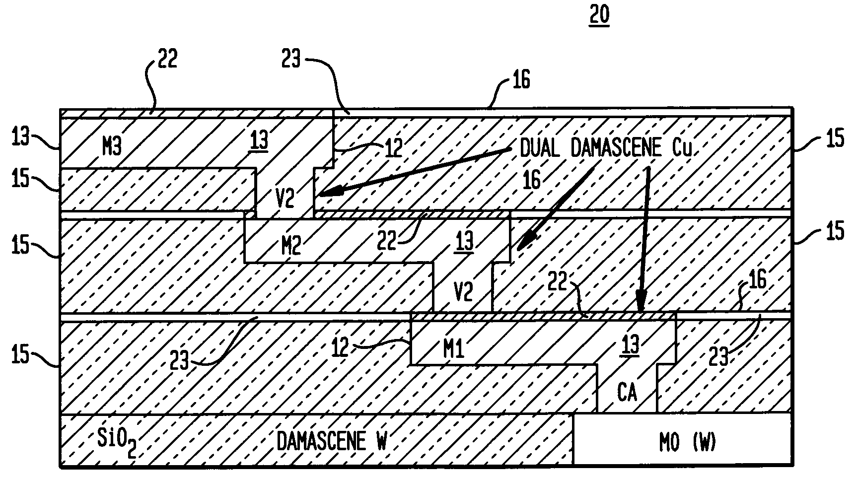
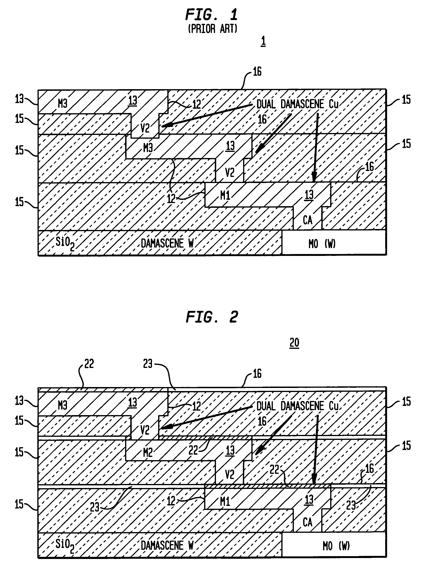
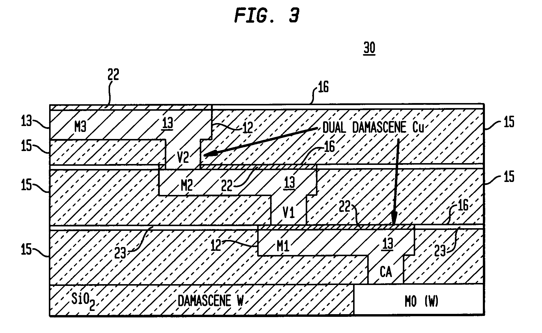
[0019]A schematic of a cross-sectional view of conventional Cu interconnections is shown in FIG. 1. The electronic structure 1 contains a typical three-level Cu dual-damascene interconnection. The adhesion / diffusion metal liner (e.g. TaN / Ta, TaTi) 12 and a body of Cu conductor 13, insulator (SiO2, low dielectric constant materials) 15 and adhesion / diffusion insulator layer (e.g. SiNx) 16 which are the fundamental layers for the damascene structure are shown. The local interconnection W M0 is connected to the first level Cu lines M1 by the inter-level vias CA. The second level Cu M2 line are connected to M1 and the third level Cu line M3 by V1 and V2 vias, respectively, embedded within the under layer dielectric without causing an electric short circuit between the Cu lines.

[0020]The subjects of electromigration, stress-induced migration, corrosion and adhesion in on-chip Cu interconnections are all related to the properties of the top surface of the Cu damascene lines. The fast Cu s...


PUM

PropertyMeasurementUnit
thicknessaaaaaaaaaa
temperatureaaaaaaaaaa

Abstract

Disclosed is a procedure to coat the free surface of Cu damascene lines by a 1-5 nm thick element prior to deposition of the inter-level dielectric or dielectric diffusion barrier layer. The coating provides protection against oxidation, increases the adhesion strength between the Cu and dielectric, and reduces interface diffusion of Cu. In addition, the thin cap layer further increases electromigration Cu lifetime and reduces the stress induced voiding. The selective elements can be directly deposited onto the Cu embedded within the under layer dielectric without causing an electric short circuit between the Cu lines. These chosen elements are based on their high negative reduction potentials with oxygen and water, and a low solubility in and formation of compounds with Cu.

Description

BACKGROUND OF THE INVENTION[0001]1. Field of the Invention[0002]This invention relates to the general field of copper-based interconnections for integrated circuits.[0003]2. Description of the Prior Art[0004]The industry need for increased integrated circuit (IC) chip performance beyond 0.25 μm technology in conjunction with decreasing feature size is causing migration of interconnect systems to lower resistivity Cu based-conductors. Modem commercial Cu IC chips, which usually contain 4 to 8 levels of Cu interconnections, are generally fabricated by a single and / or dual damascene process. The two most important on-chip interconnection reliability issues are electromigration and stress induced voiding in the Cu interconnect circuit elements. Electromigration in copper metallization for IC chips has been extensively studied. Electromigration and stress induced voiding are the motion of atoms by diffusion in an electrical field and stress gradient, respectively. When an interconnect is...

Claims


Application Information

Patent Timeline
Patent Type & Authority Patents(United States)
IPC IPC(8): H01L23/48H01L23/52H01L29/40
CPCH01L21/76829H01L21/76849H01L23/53238H01L23/53295H01L2924/0002H01L2924/3011H01L2924/00
Inventor BRULEY, JOHNCARRUTHERS, ROY A.GIGNAC, LYNNE MARIEHU, CHAO-KUNLINIGER, ERIC GERHARDMALHOTRA, SANDRA GUYROSSNAGEL, STEPHEN M.
Owner GLOBALFOUNDRIES US INC
Why Eureka
Try Eureka