Molding technique for fabrication of optoelectronic devices

Inactive Publication Date: 2007-08-07
AERIS CAPITAL SUSTAINABLE IP
View PDF39 Cites 162 Cited by
  • Summary
  • Abstract
  • Description
  • Claims
  • Application Information

AI Technical Summary

Benefits of technology

[0021]Embodiments of the present invention provide new and useful optoelectronic devices including photovoltaic

Problems solved by technology

Higher efficiencies were not obtained since the phase separating network was essentially random with isolated “islands”, phases/features that were too large (10-100 nm) and poor connectivity with the respective electrodes.
The totally random and highly inefficient placement of the nanorods lowered the solar cell efficiency from what would be expected if the exciton-separating network was ordered and interconnected on the desired 10-nm scale.
The interpenetrating network obtained this way is still not on the optimal size scale (about 10 nm) for these polymers.
These prior art devices are limited by the extent to which excitons can be harvested to perform useful work.
First, in cells created with semiconducting nanorods, the nanorods within the solar cells were randomly arranged within a medium of conducting polymer. Since many nanorods were only partially aligned and large clusters of nanorods (interspersed with areas of few rods) were present in the devices, many excitons traveling through the active layers of these devices did not reach an electron affinity junction before spontaneously recombining. As the spacing of the nanorods was random, some areas of the device had many nanorods within 10 nm of one another, while many other areas of the device had no nanorods at all within 10 nm of one another (resulting in “dead” absorption space). This factor decreased

Method used


Image

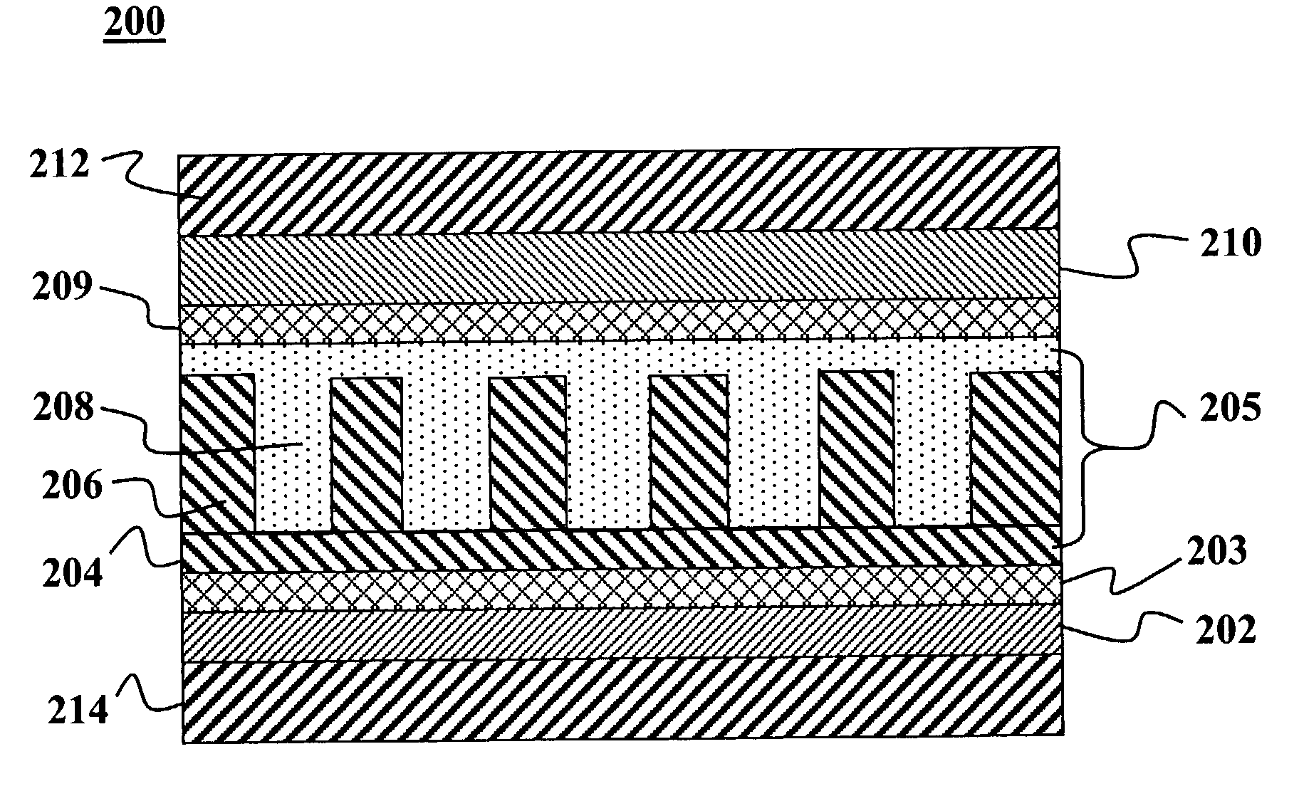
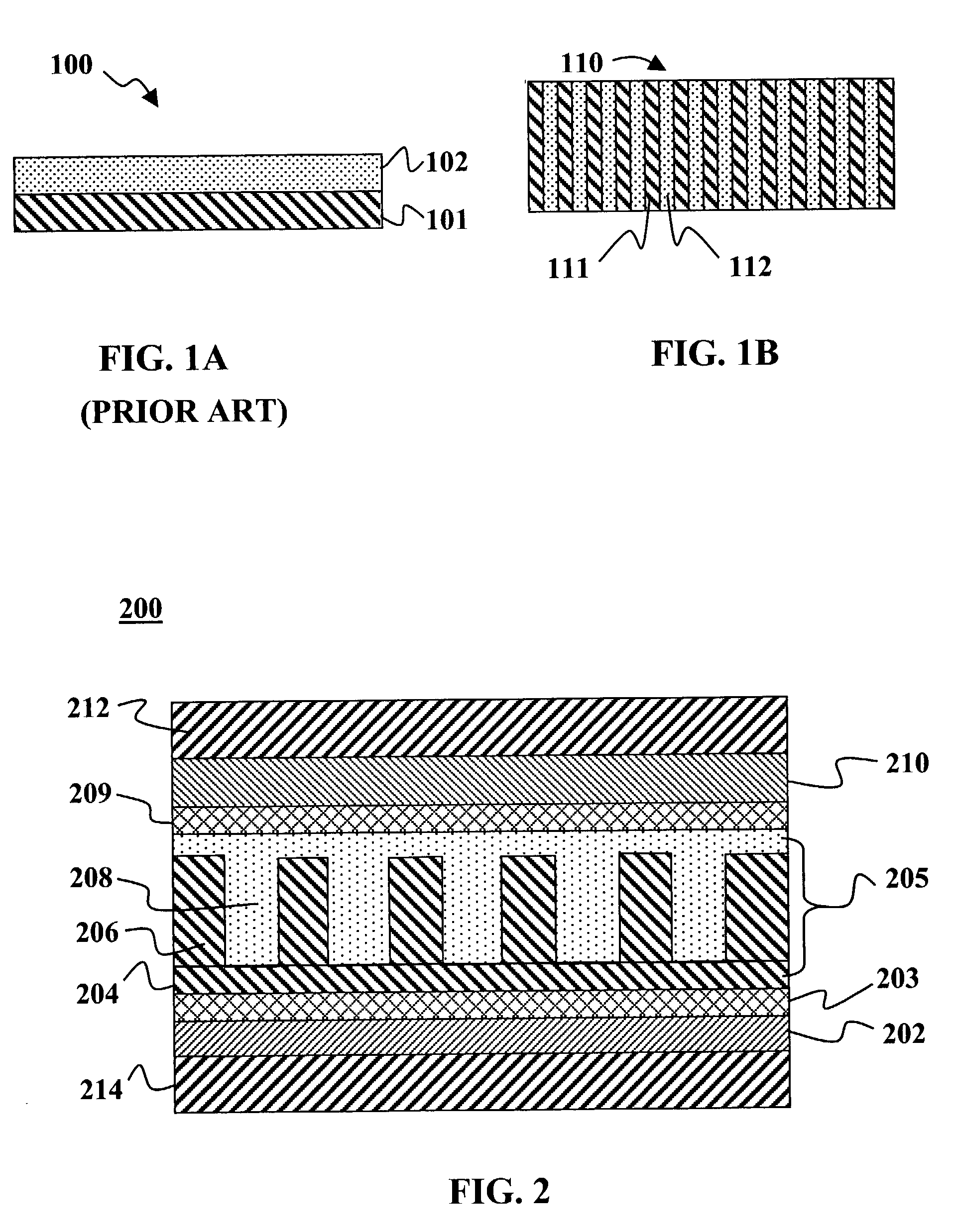
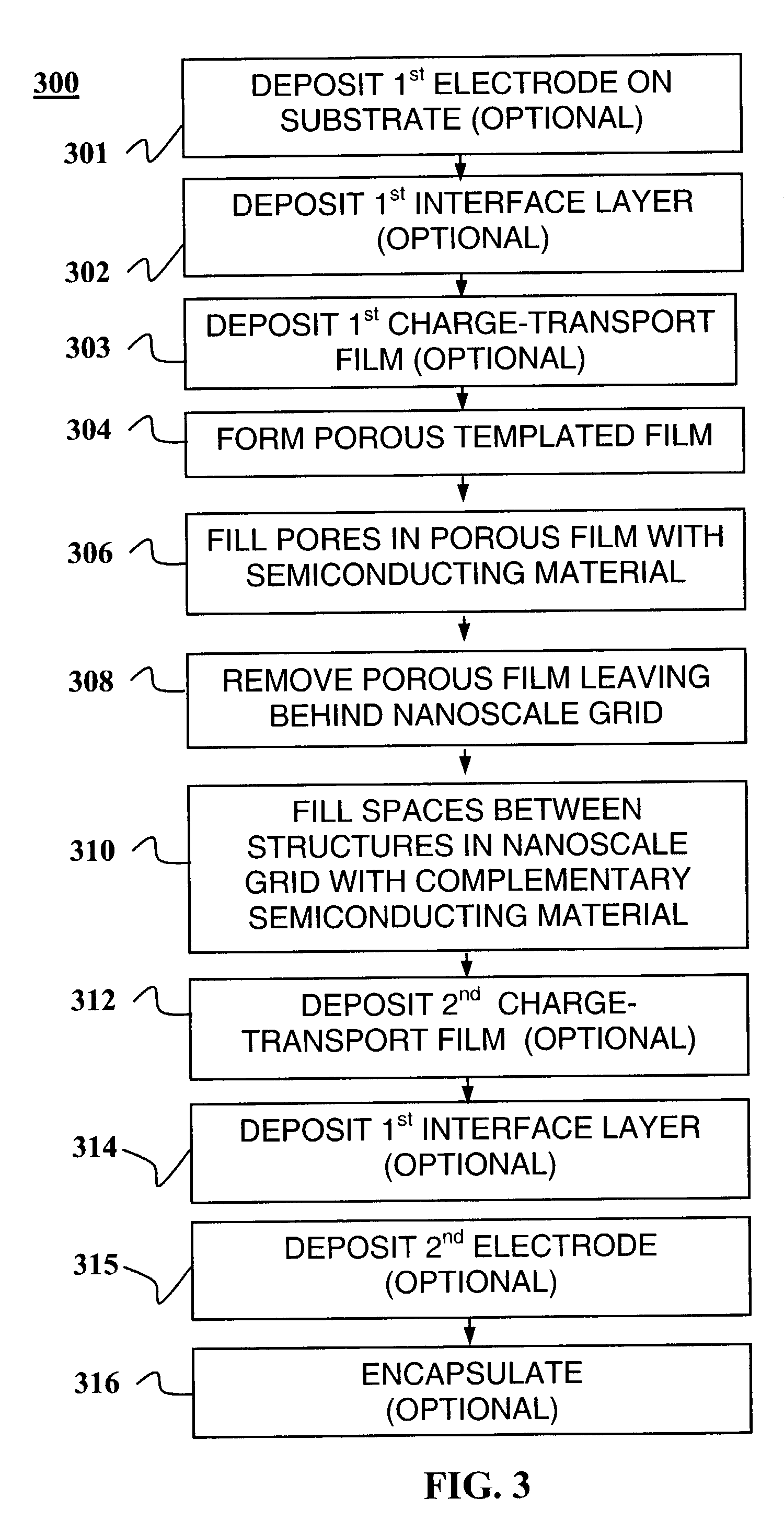
  • Molding technique for fabrication of optoelectronic devices
  • Molding technique for fabrication of optoelectronic devices
  • Molding technique for fabrication of optoelectronic devices

Examples


Embodiment Construction

Contents

I. Glossary

II. General Overview

III. Solar Cell Device Architecture

IV. Alternative Embodiments

V. Conclusion

I. GLOSSARY

[0032]The following terms are intended to have the following general meanings as they are used herein:

[0033]Device: An assembly or sub-assembly having one or more layers of material.

[0034]Semiconductor: As used herein, semiconductor generally refers to a material characterized by an electronic bandgap typically between about 0.5 eV and about 3.5 eV.

[0035]Hole-Acceptor, Electron-Acceptor: In the case of semiconductor materials, hole-acceptor and electron-acceptor are relative terms for describing charge transfer between two materials. For two semiconductor materials wherein a first material has a valence band edge or highest occupied molecular orbital (HOMO) that is higher than the corresponding valence band edge or HOMO for a second material, and wherein the first material has a conduction band edge or lowest unoccupied molecular orbital (LUMO) that is higher ...


PUM


Abstract

Charge splitting networks for optoelectronic devices may be fabricated using a nanostructured porous film, e.g., of SiO2, as a template. The porous film may be fabricated using surfactant temptation techniques. Any of a variety of semiconducting materials including semiconducting metals and metal oxides (such as TiO2, CdSe, CdS, CdTe, or CuO) may be deposited into the pores of the porous template film. After deposition, the template film may be removed by controlled exposure to acid or base without disrupting the semiconducting material leaving behind a nanoscale network grid. Spaces in the network grid can then be filled with complementary semiconducting material, e.g., a semiconducting polymer or dye to create a exciton-splitting and charge transporting network with superior optoelectronic properties for an optoelectronic devices, particularly photovoltaic devices.

Description

CROSS-REFERENCE TO AN EARLIER FILED APPLICATION[0001]This application claims priority to U.S. Provisional Patent Application 60 / 390,904, filed Jun. 22, 2002, the entire disclosures of which are incorporated herein by reference. This application is also a continuation-in-part of U.S. patent application Ser. No. 10 / 290,119 to Brian Sager et al, entitled “OPTOELECTRONIC DEVICE AND FABRICATION METHODS”, filed Nov. 5, 2002, the entire disclosures of which are incorporated herein by reference.FIELD OF THE INVENTION[0002]This invention generally relates to optoelectronic devices and more particularly to photovoltaic, e.g., solar cell, devices.BACKGROUND OF THE INVENTION[0003]Optoelectronic devices interact with radiation and electric current. Solar cells are a particular example of a useful class of optoelectronic devices. Organic solar cell technology has been actively pursued in the research community due to its promise of lower cost, easier manufacturability, and other potential advanta...

Claims


Application Information

Patent Timeline
IPC IPC(8): H01L21/00
CPCB82Y30/00H01L31/0352H01L31/03529H01L51/0015H01L51/4253H01L51/422Y02E10/549H10K71/211H10K30/15H10K30/30
Inventor ROSCHEISEN, MARTIN R.SAGER, BRIAN M.FIDANZA, JACQUELINEPETRITSCH, KLAUSMILLER, GREGORY A.YU, DONG
Owner AERIS CAPITAL SUSTAINABLE IP
Why Eureka
Try Eureka