

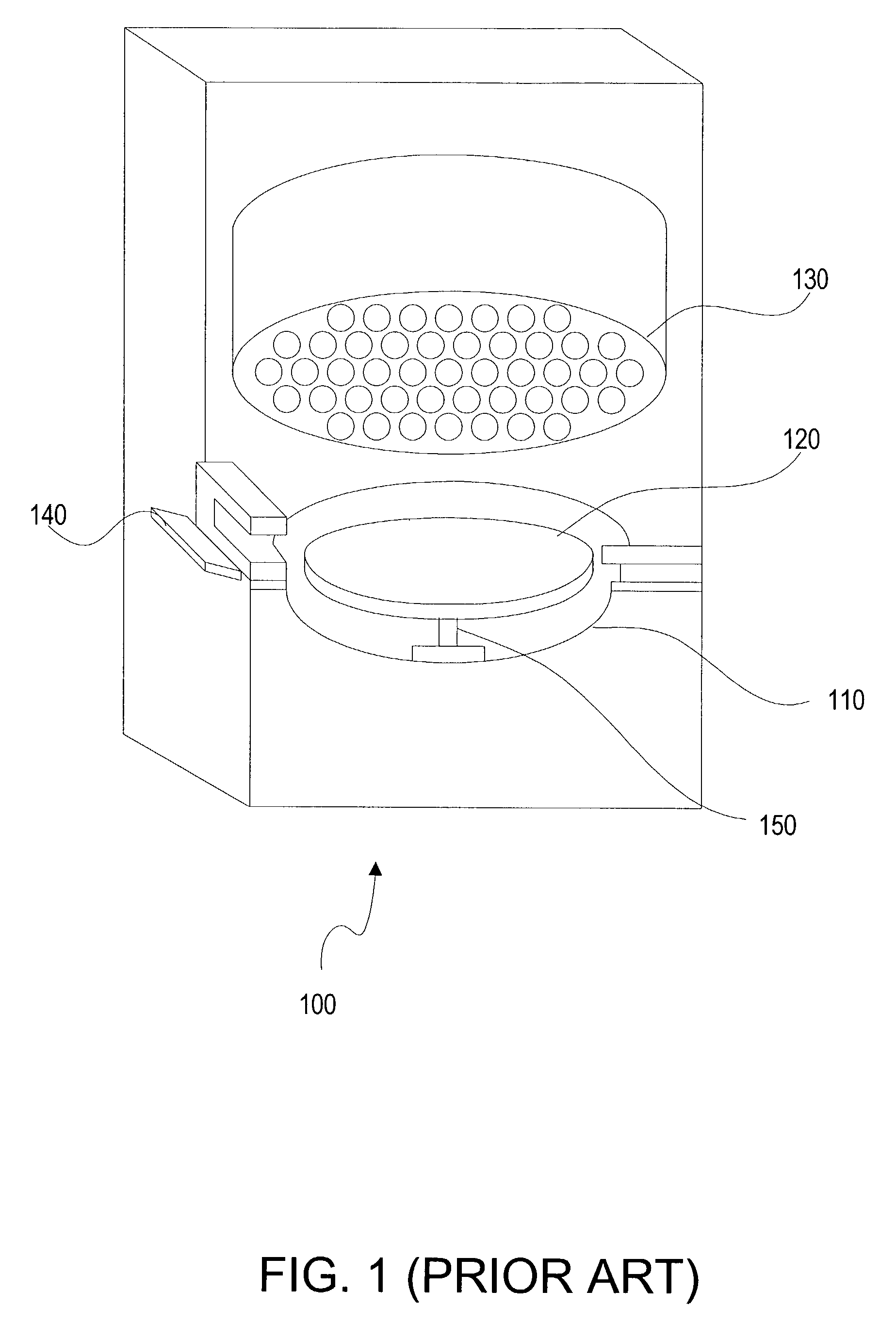
Vacuum thermal annealer
a vacuum thermal furnace and annealer technology, applied in the field of furnaces, can solve the problems of difficult control of temperature, increased difficulty in manufacturing semiconductor devices, and high difficulty in forming semiconductor devices, so as to achieve the effect of sweeping the substrate, reducing the flow of heated gas, and increasing the pressure in the process chamber
- Summary
- Abstract
- Description
- Claims
- Application Information
AI Technical Summary
Benefits of technology
Problems solved by technology
Method used
Image

Examples
Embodiment Construction
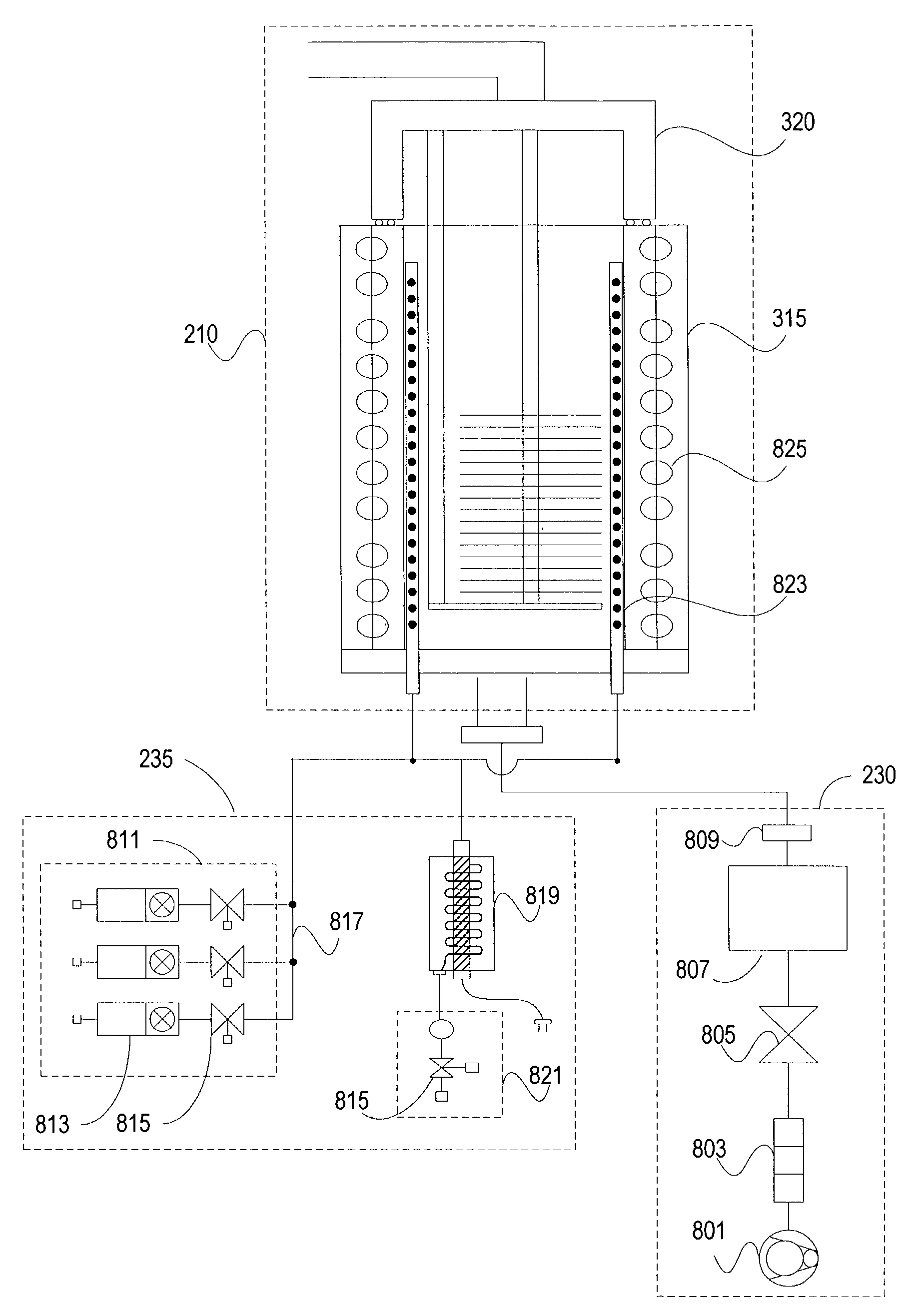
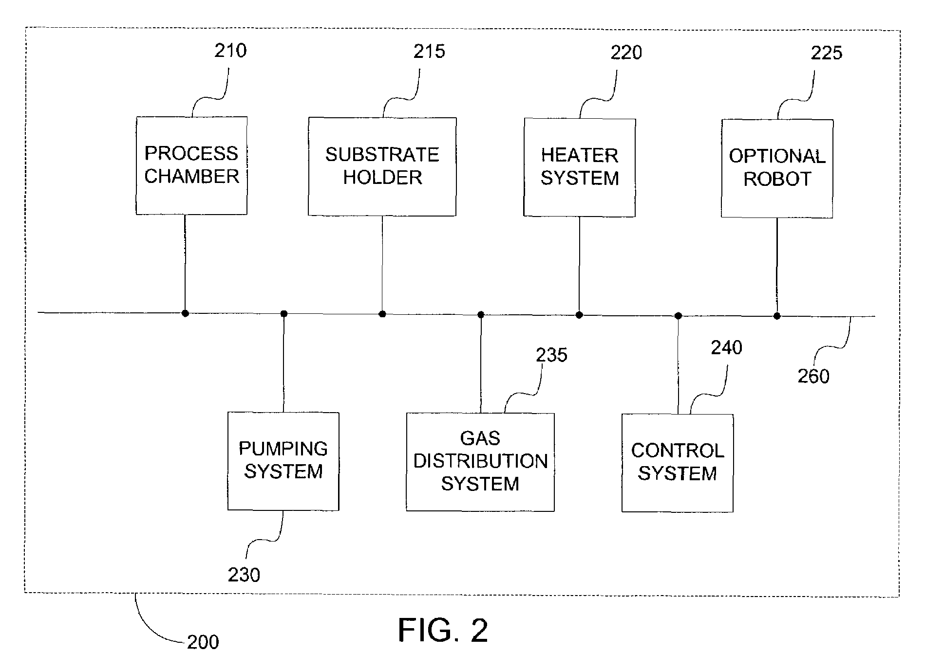
[0033]FIG. 2 is a block diagram showing components of an exemplary vacuum thermal annealing furnace 200. The vacuum thermal annealing furnace 200 includes a process chamber 210, a substrate holder 215, a heater system 220, an optional robot 225, a pumping system 230, a gas distribution system 235, a control system 240, and a bus 260 which couples all of these components together. The control system 240 is hardware and / or software-based, which is coupled to some or all the other components in the vacuum thermal annealer 200. The substrate holder 215 (also referred to as a substrate mantle) is used to hold wafers or other substrates during an annealing process, and is constructed from materials with favorable heat transfer properties, such as aluminum or zirconia. Additionally, the substrate holder 215 can be interchanged with a substrate holder made of different materials in order to satisfy needs of a particular annealing application.
[0034]The control system 240 provides a central p...
PUM
| Property | Measurement | Unit |
|---|---|---|
| temperature | aaaaa | aaaaa |
| pressure | aaaaa | aaaaa |
| diameter | aaaaa | aaaaa |
Abstract
Description
Claims
Application Information