Integrated photonic-electronic circuits and systems

a photonic-electronic circuit and integrated circuit technology, applied in the field of integrated circuits, can solve the problems of physical inability to support such data rates at acceptable power consumption levels, unacceptable packaging and/or cost constraints, and significant bottlenecks in communication between networks, devices and components of devices, etc., to achieve the effect of enhancing flexibility and functionality

Inactive Publication Date: 2007-08-21
CISCO TECH INC
View PDF1 Cites 85 Cited by
  • Summary
  • Abstract
  • Description
  • Claims
  • Application Information

AI Technical Summary

Benefits of technology

[0004]Integrated photonic-electronic circuit chips having a photonic portion and an electronic portion may be implemented using group IV containing materials. Optical signal transmission and / or reception capabilities may be implemented on the same chip as electronic logic devices. In some cases, the electronic portion may be used to configure and / or manage the optical portion. In some cases, the integrated photonic-electronic circuit chips may be remotely and / or automatically reconfigurable; some implementations may be introspective. Novel systems may be created by optically coupling two or more integrated photonic-electronic circuit chips. Optionally, integrated photonic-electronic chips may further comprise electrical connections for transmitting and / or receiving electrical signals, providing additional flexibility and functionality. An integrated photonic-electronic design automation tool supports the design, definition and verification of circuit systems with integrated photonic-electronic chips. A multi-chip module (MCM) layout system supports the layout and optimization of MCMs that include photonic-electronic chips.

Problems solved by technology

Traditional wire-based connections, however optimized, have proven physically incapable of supporting such data rates at acceptable power consumption levels and / or without unacceptable constraints on packaging and / or cost.
As a result, electrical wiring has become a significant bottleneck in communication between networks, devices and components in devices.

Method used


Image

  • Integrated photonic-electronic circuits and systems
  • Integrated photonic-electronic circuits and systems
  • Integrated photonic-electronic circuits and systems

Examples


Embodiment Construction

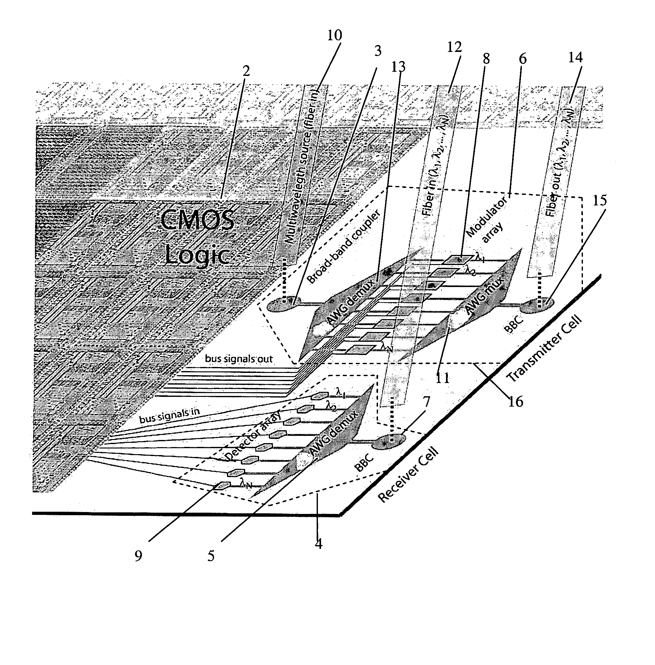
[0025]FIG. 1 illustrates an example of an integrated photonic-electronic circuit according to the current invention. In this example, electronic circuit portion 2 is a Complementary Metal Oxide Semiconductor (CMOS) logic module. In other examples, the electronic circuit portion may comprise a variety of electronic components comprising a layer of group IV semiconductor materials such as silicon (Si) and / or germanium (Ge). In some cases, both silicon and germanium may be present; for example, some electronic components may comprise silicon-germanium (Si—Ge) solid solutions and / or superlattices comprising silicon and germanium. Examples of electronic components include, but are not limited to, processors, memory modules, analog circuits, Radio Frequency (RF) circuits, memory controllers, One-Time Programmable (OTP) and / or reconfigurable Programmable Logic Devices (PLD), Complex Programmable Logic Devices (CPLD) and / or Field Programmable Gate Arrays (FPGA). Furthermore, the electronic ...


PUM


Abstract

Photonic interconnect reconfigurably couples integrated circuits such as microprocessor, memory or other logic components. Detector, modulator, broad-band coupler and waveguide elements provide transmit and receive capability on CMOS substrate. Computer-implemented design software and reusable component library automate photonic and circuit design and simulation for manufacturability.

Description

CROSS-REFERENCE TO RELATED APPLICATIONS[0001]This application is a divisional of application Ser. No. 10 / 758,561 filed Jan. 14, 2004 now U.S. Pat. No. 7,251,386, which claims a benefit of priority from U.S. Non-provisional application Ser. No. 10 / 606,297 filed Jun. 24, 2003, the entire contents of which is hereby expressly incorporated by reference.FIELD OF INVENTION[0002]Invention relates to integrated circuits, particularly circuits with electronic and photonic portions on the same chip.BACKGROUND OF INVENTION[0003]The rapid expansion in the use of the Internet and data-intensive applications such as machine-vision, video conferencing, and real-time image processing have created a need for communication conduits and devices capable of handling large amounts of data at very high speeds. These applications might need data rates with an order of magnitude of a terabyte per second. Traditional wire-based connections, however optimized, have proven physically incapable of supporting su...

Claims


Application Information

Patent Timeline
Patent Type & Authority Patents(United States)
IPC IPC(8): H01L21/00
CPCB82Y20/00G02B6/12004G02B6/12019G02B6/1225H04B10/25G02B6/43
Inventor DICKINSON, ALEXANDER G.GUNN, III, LAWRENCE C.NECHES, PHILIP M.HUANG, ANDREW SHANE
Owner CISCO TECH INC
Why Eureka
Try Eureka