
Flat panel display device with surfaces of cathodes and control electrodes lying in the same flat plane

a display device and control electrode technology, applied in the manufacture of electric discharge tubes/lamps, tubes with screens, discharge tubes luminescnet screens, etc., can solve the problems of increasing the size of cathodes, increasing the power consumption necessary to obtain the required light emission intensity, and inability to prevent the drive circuit from becoming complicated, etc., to achieve low control voltage, high efficiency, and easy manufacture

Inactive Publication Date: 2007-08-21
PANASONIC LIQUID CRYSTAL DISPLAY CO LTD +1
View PDF9 Cites 5 Cited by
  • Summary
  • Abstract
  • Description
  • Claims
  • Application Information

AI Technical Summary

Benefits of technology

[0012]Accordingly, it is an object of the present invention to provide a flat panel display device which produces an electron emission of high efficiency at a low voltage by setting the control electrode current to an extremely small value using diamond, carbon nanotubes, micro carbon fibers or the like as cathodes.
[0013]To achieve the above-mentioned object, the present invention adopts a driving method in which an electric field necessary for electron emission is applied in response to a potential difference between cathodes and anodes which constitute a light emitting surface, and the electron emission is controlled by cutting off the electric field in response to a voltage applied to the control electrodes. More particularly, the present invention adopts a structure in which the control electrodes and the cathodes are formed on substantially the same plane. Due to such a structure, it is possible to obtain a flat panel display device of high efficiency and which employs a low control voltage and can be manufactured readily.

Problems solved by technology

Accordingly, it is necessary to change over the anode voltage, which is a high voltage of several hundreds V or several kV necessary for making the phosphors emit light, and, hence, it is impossible to prevent the drive circuit from becoming complicated.
Since the pull-out electrode current does not contribute to the light emission at all, there is a high possibility that the power consumption necessary for obtaining the required light emitting intensity will be increased.
However, since the driving voltage necessary for turning on or off the electrons emitted from the cathodes is lowered, the size of the cathodes is limited, and thus it is difficult to increase the width of branch portions which connect the cathodes and the cathode lines.
Accordingly, it is difficult to fill a material which ensures electric conductivity, thus eventually giving rise to a possibility that an electrical contact failure arises.

Method used


Image

  • Flat panel display device with surfaces of cathodes and control electrodes lying in the same flat plane
  • Flat panel display device with surfaces of cathodes and control electrodes lying in the same flat plane
  • Flat panel display device with surfaces of cathodes and control electrodes lying in the same flat plane

Examples


first embodiment

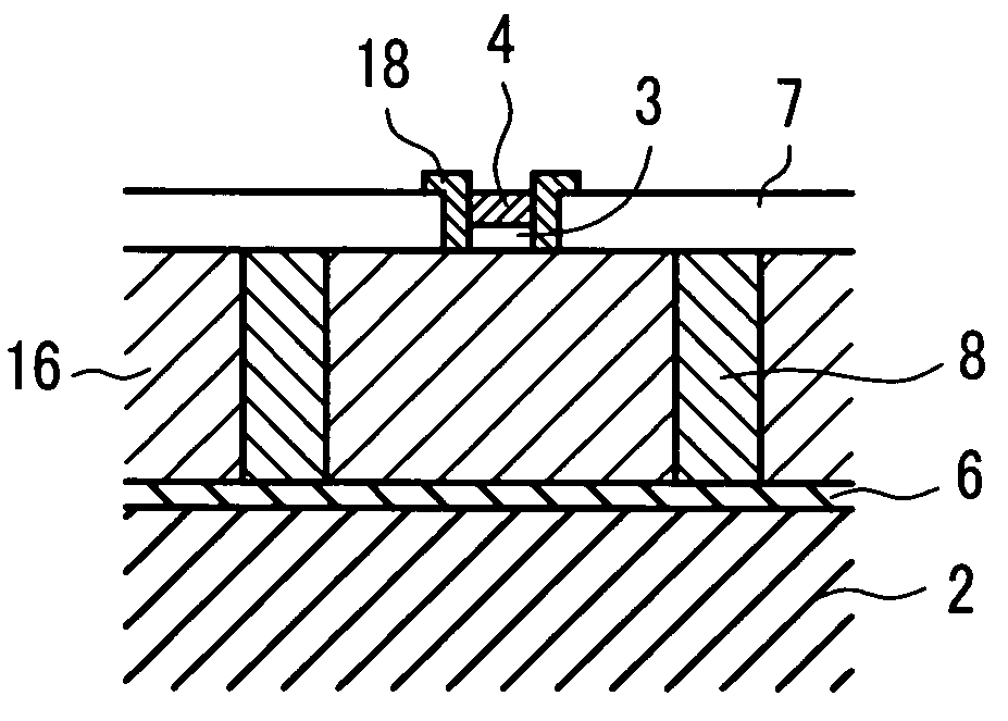
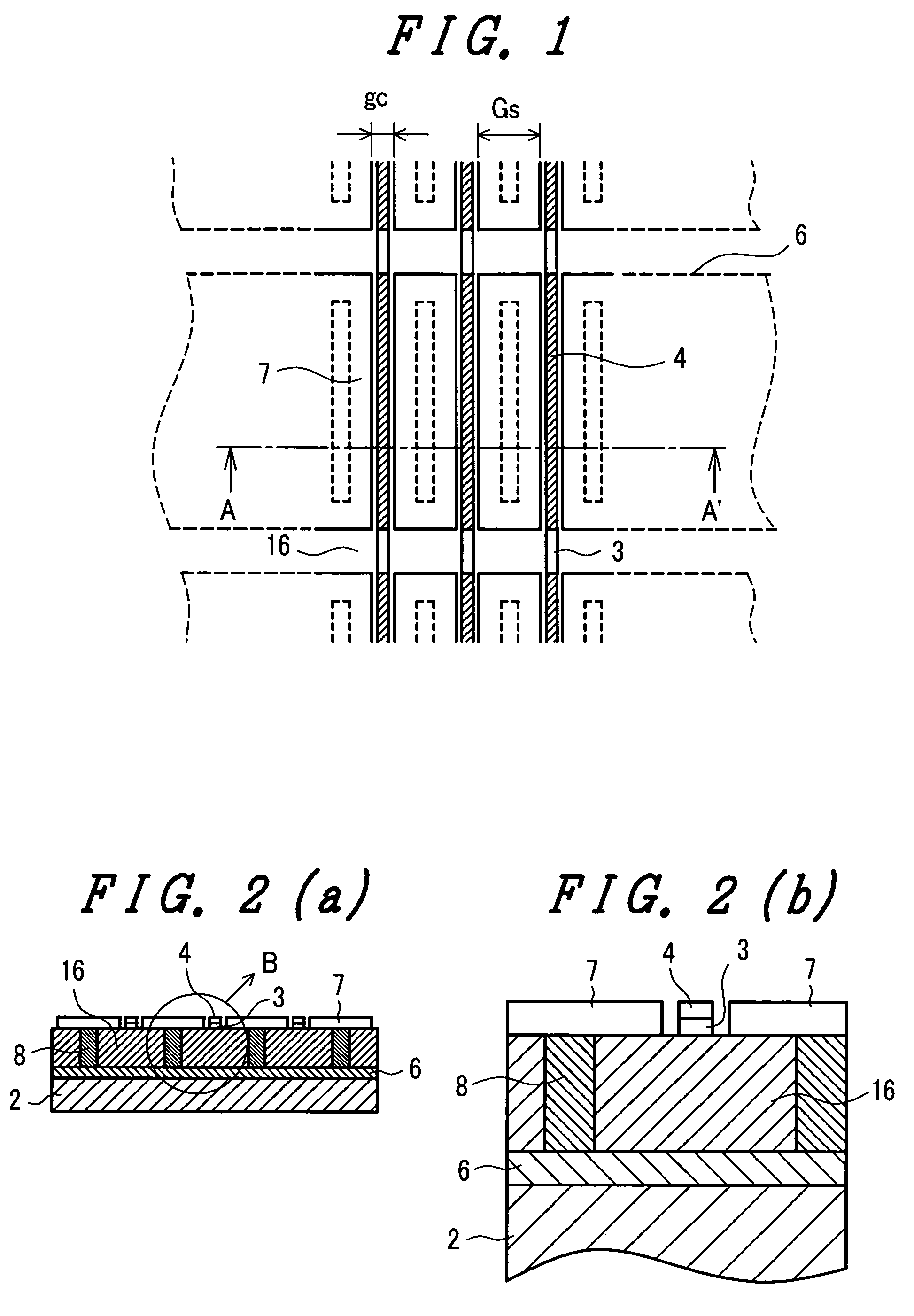
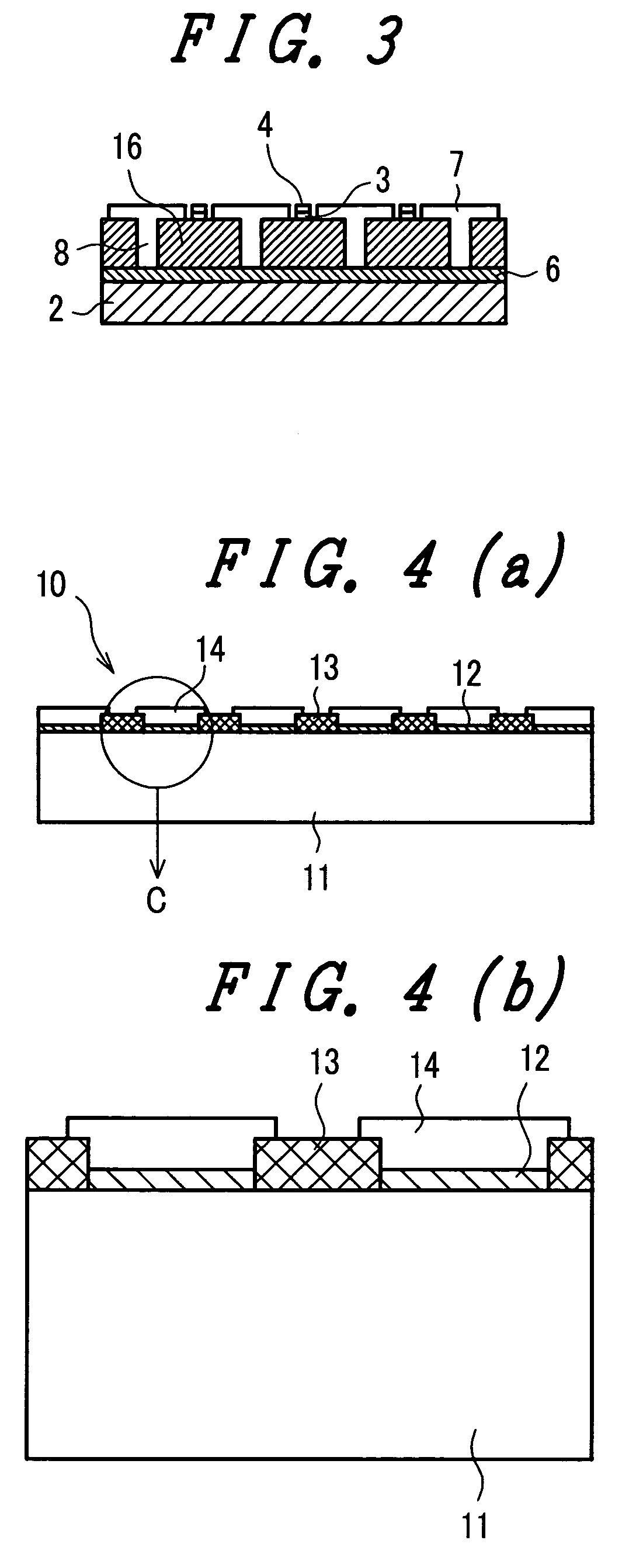
[0037]A first embodiment will be explained in conjunction with FIG. 1 to FIG. 6. FIG. 1 is a plan view of part of a first panel showing some control electrodes and some cathodes of a flat panel display device according to the present invention, having an electrode structure in which the control electrodes and the cathodes are arranged on substantially the same plane (the first panel also will be referred to as the electron beam source panel, hereinafter).

[0038]In this embodiment, control electrodes 7 and cathodes 4 are formed on a substrate 2 which constitutes an electron beam source panel 1, the electron beam source panel 1 constituting a first panel of a flat panel display device, as shown in FIG. 6. Here, this embodiment has an electrode structure in which the control electrodes 7 and cathodes 4 are substantially formed on the same plane. The electron beam source panel 1 is configured by forming the cathodes 4, the control electrodes 7 and the like on the substrate 2, which is pr...

second embodiment

[0047]A second embodiment of the present invention will be explained in conjunction with FIG. 7 and FIG. 8. Although the surfaces of the control electrodes 7 and the cathodes 4 are arranged substantially coplanar with each other in the above-mentioned first embodiment, even when the difference in height between the surface of the cathodes 4 and the surface of the control electrodes 7 is equal to approximately the thickness of the control electrodes 7, it is possible to obtain an advantageous effect similar to the advantageous effect obtained by the first embodiment. FIG. 7 is a cross-sectional view which substantially corresponds to FIG. 2(a) for showing the second embodiment of the present invention in which the cathodes 4 are formed on the cathode lines 3, which are simultaneously formed with the control electrodes 7. Further, FIG. 8 is a plan view similar to FIG. 1 and shows an electrode structure in which the control electrode lines 6 are formed with a narrow width.

[0048]That is...

third embodiment

[0051]A third embodiment of the present invention will be explained in conjunction with FIG. 9. FIG. 9 is a cross-sectional view similar to FIG. 2(a) showing the third embodiment of the present invention in which the control electrodes and the branch lines are integrally formed. In the above-mentioned embodiments, when it is possible to ensure a large area for the control electrodes 7 due to a large pixel pitch or the like, the branch lines 8 are not formed and the insulation layer 16 is formed while obviating regions corresponding to the branch lines 8; and, thereafter, a conductive paste is injected into the regions corresponding to the branch lines 8 at the time of forming the control electrodes 7 by printing, thus forming the structure shown in FIG. 9. Due to such a constitution, integral-type control electrodes 7′ which correspond to the branch lines 8 and the control electrodes 7 are formed.

[0052]Also, in this embodiment, it is possible to provide a flat panel type display dev...


PUM


Abstract

A structure is provided which facilitates manufacturing of a flat type image display element which includes electrodes capable of enhancing the display efficiency with an extremely small control electrode current using a cathode material which can obtain a sufficient intensity of electron emission in a low electric field. A structure is provided in which control electrodes and cathodes are formed substantially on a the plane on a first panel, while control electrode lines which electrically connect the control electrodes of a plurality of pixels are not included in the plane which is parallel to a phosphor screen panel and includes the cathodes and the control electrodes.

Description

BACKGROUND OF THE INVENTION[0001]The present invention relates to a flat panel display device which includes electron beam sources having cathodes which emit electrons in response to an electric field and a phosphor screen which is excited by the electrons emitted from the electron beam sources; and, more particularly, the invention relates to a flat panel display device which uses a carbon-based material, such as carbon nanotubes, micro carbon fibers, diamond or the like, as cathodes which emit electrons with a low electric field.[0002]Recently, as represented by diamond, carbon nanotubes or the like, electron emission materials have been found which can produce an emission of sufficient electrons with an extremely low electric field as compared to field-emission-type electron sources which use a conventional metal material as a main material. A flat panel display device which uses such an electron emission material as a material of the cathodes is described in patent literature 1 ...

Claims


Application Information

Patent Timeline
Patent Type & Authority Patents(United States)
IPC IPC(8): H01J63/06H01J29/04H01J1/304H01J1/62H01J29/02H01J29/48H01J31/12H01J63/04
CPCB82Y10/00H01J29/481H01J31/127H01J2201/30469
Inventor YAGUCHI, TOMIOMUNEYOSHI, TAKAHIKOOKAI, MAKOTOHAYASHI, NOBUAKI
Owner PANASONIC LIQUID CRYSTAL DISPLAY CO LTD
Learn More