Integrated semiconductor memory with clock generation

a technology of integrated semiconductor memory and clock generation, which is applied in the direction of generating/distributing signals, pulse techniques, pulse characteristics measurements, etc., can solve the problems of reduced sensitivity of the differential amplifier with regard to level fluctuations of the external clock signal at its input terminal, uncontrolled switching behavior of the internal chip logic, and so on. , to achieve the effect of shortening the sensitivity time of the clock generator circuit, reducing the sensitivity of the differential amplifier with regard to level fluctuations of the external clock

Inactive Publication Date: 2007-08-21
POLARIS INNOVATIONS LTD
View PDF13 Cites 6 Cited by
  • Summary
  • Abstract
  • Description
  • Claims
  • Application Information

AI Technical Summary

Benefits of technology

[0017]In accordance with one development of the integrated semiconductor memory according to the invention the control circuit can be driven by a first external clock signal and by a second external clock signal. In this case, the first external clock signal has a higher signal / noise ratio than the second external clock signal. According to the invention, the control circuit is designed in such a way that it shortens the sensitivity time of the clock generator circuit in the case of driving with the first external clock signal and lengthens the sensitivity time of the clock generator circuit in the case of driving with the second external clock signal.
[0018]In accordance with one development of the integrated semiconductor memory according to the invention, the first external clock signal has a higher frequency and phase stability than the second external clock signal. The control circuit is designed in such a way that it shortens the sensitivity time of the clock generator circuit in the case of driving with the first external clock signal and lengthens the sensitivity time of the clock generator circuit in the case of driving with the second external clock signal.
[0019]In the case of driving of the integrated semiconductor memory with an external clock signal which exhibits high quality, that is to say is distinguished by a large signal / noise ratio or a high frequency and phase stability, the sensitivity time of the clock generator circuit is shortened by the control circuit. The clock generator circuit thus reacts more rapidly to fluctuations of the external clock signal. This means that it generates a low internal clock signal level, for example, if it is driven by a very momentary fluctuation of the external clock signal that lies below its sensitivity level. Conversely, it generates a high internal clock signal level if it is driven by a momentary fluctuation of the external clock signal level that lies above its sensitivity level. Consequently, a high-frequency, non-noisy external clock signal can be converted into a high-frequency internal clock signal.
[0020]If the integrated semiconductor memory is driven by an external clock signal of poor quality, that is to say for example by an external clock signal with a small signal / noise ratio or a low frequency and phase stability, then the control circuit lengthens the sensitivity time of the clock generator circuit. This ensures that the clock generator circuit does not follow undesired level fluctuations, such as occur in the case of a noisy external clock signal, with internal clock signal level changes. Only longer-term changes in the external clock signal level above or below its sensitivity level are converted into internal clock signal level changes by the clock generator circuit. This prevents a high-frequency noise superposed on the external clock signal from leading to an undesired switching behavior of the clock generator circuit.
[0021]In particular when testing an integrated semiconductor memory, the latter is driven with an external clock signal of poor quality by a test system. This external clock signal is generally distinguished by a low frequency besides the small signal / noise ratio and the low frequency and phase stability. In accordance with another embodiment of the invention, therefore, the control circuit evaluates the external clock signal by which it is driven with regard to the frequency of said signal. If it is driven by an external clock signal with a low frequency, that is to say for example by the noisy external clock signal that is prescribed by a tester, it lengthens the sensitivity time of the clock generator circuit. High-quality clock signals are generally generated with a high frequency by a memory controller, for example. According to the invention, therefore, the control circuit is designed in such a way that it shortens the sensitivity time of the clock generator circuit in the case of driving with an external clock signal having a high frequency.

Problems solved by technology

The input noise (jitter) of the external clock signal thereby leads to an uncontrolled switching behavior of the internal chip logic.
However, the disadvantage of this solution to the problem lies in the positive feedback, which leads to a reduced sensitivity of the differential amplifier with regard to level fluctuations of the external clock signal at its input terminals E10a and E10b.
It is also disadvantageous that the so-called duty cycle of the clock generator circuit, which characterizes the ratio of high / low times becomes highly process-dependent as a result of the positive feedback.
The duty cycle for weak or very high-frequency external clock signals is considerably impaired as a result.

Method used


Image

  • Integrated semiconductor memory with clock generation
  • Integrated semiconductor memory with clock generation
  • Integrated semiconductor memory with clock generation

Examples


first embodiment

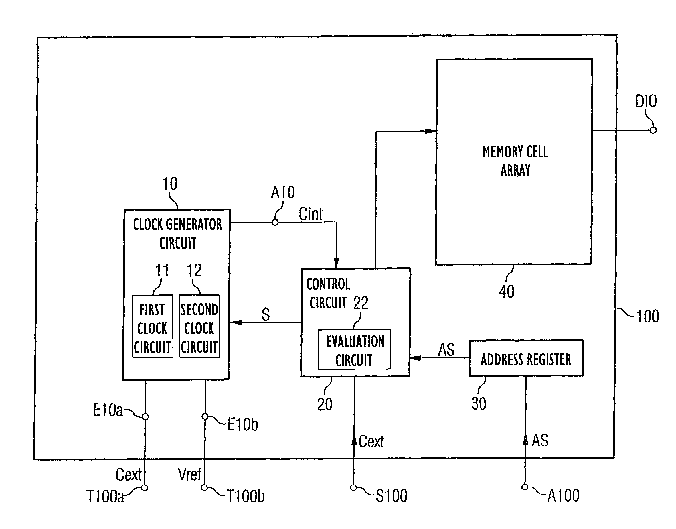
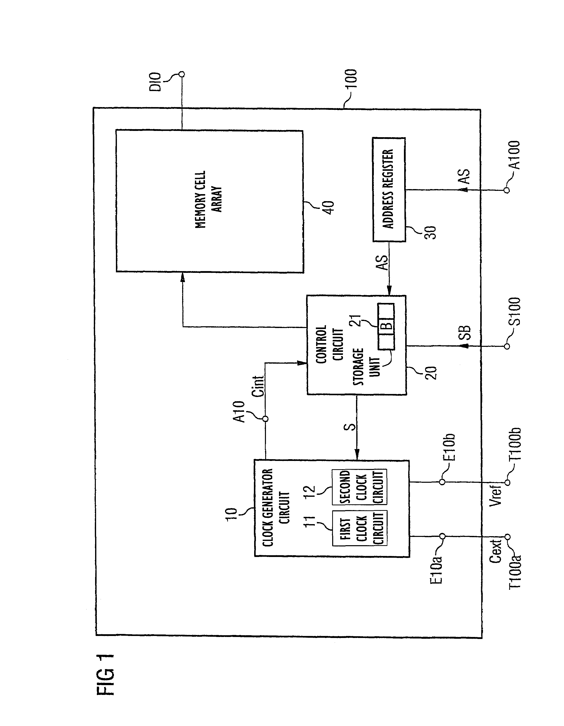
[0036]FIG. 1 shows an integrated semiconductor memory for generating an internal clock signal according to the invention. The integrated semiconductor memory has a clock generator circuit 10 and a control circuit 20 besides the address register 30 and the memory cell array 40. The clock generator circuit 10 is connected via a first input terminal E10a and a second input terminal E10b to an external clock terminal T100a for application of an external clock signal Cext and via a second input terminal E10b to a clock terminal T100b of the integrated semiconductor memory for application of a sensitivity level Vref. The clock generator circuit 10 comprises a first clock circuit 11 and a second clock circuit 12.

[0037]The first clock circuit 11 has a shorter sensitivity time that the second clock circuit 12. Since the sensitivity time is that time for which the clock generator circuit 10 must be driven at least with a high or low level of the external clock signal in order, on the output s...

second embodiment

[0043]FIG. 2 shows an integrated semiconductor memory for generating the internal clock signal Cint. The integrated semiconductor memory has a clock generator circuit 10 connected, via a first input terminal E10a, to a clock terminal T100a for application of an external clock signal Cext and, via a second input terminal E10b, to a clock terminal T100b for application of a sensitivity level Vref. The clock generator circuit 10 has the first clock circuit 11 already described in FIG. 1 and the second clock circuit 12, the first clock circuit 11 having a shorter sensitivity time TE than the second clock circuit 12. In order to generate the internal clock signal Cint at the output terminal A10 of the clock generator circuit 10, it is possible optionally to activate the first clock circuit 11 or the second clock circuit 12. The activation of the first or second clock circuit is effected by driving the clock generator circuit 10 with a first or second state of a control signal S generated...

third embodiment

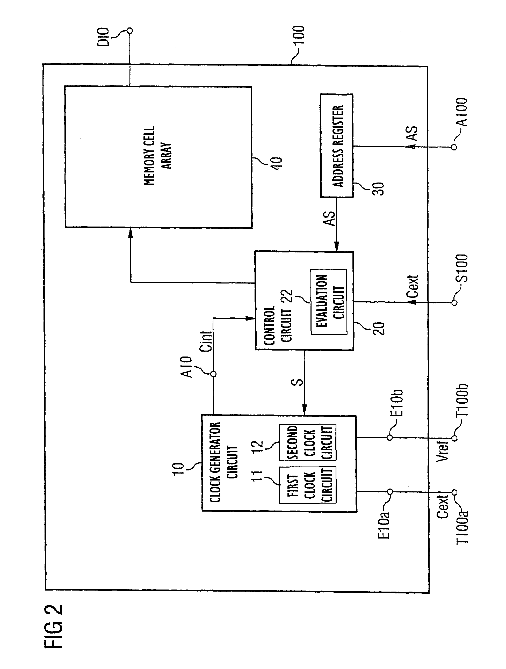
[0046]FIG. 3 shows an integrated semiconductor memory for generating the internal clock signal Cint. The integrated semiconductor memory has a control circuit 20, to which an external clock signal CLK can be fed via a first control terminal S100a and a complementary external clock signal / CLK with respect thereto can be fed via a second control terminal S100b.

[0047]In the embodiment of FIG. 3, then, the control circuit 20 is driven by an external clock signal comprising two individual signals exhibiting mutually complementary behavior. The control circuit 20 has the evaluation circuit 22—already described in FIG. 2—for evaluating the signal / noise ratio and / or the frequency and / or the frequency and phase stability of the external clock signal.

[0048]The clock generator circuit 10 is connected, via a first input terminal E10a, to a first clock terminal T100a for application of the external clock signal CLK and, via a second input terminal E10b, to a second clock terminal T100b of the ...


PUM


Abstract

An integrated semiconductor memory includes a clock generator circuit driven by an external clock signal and a control circuit driven by the external clock signal. The clock generator circuit generates an internal clock signal with a first level if the external clock signal level lies above a sensitivity level of the clock generator circuit for at least the duration of a sensitivity time of the clock generator circuit, and generates the internal clock signal with a second level if the external clock signal level lies below the sensitivity level for at least the duration of the sensitivity time of the clock generator circuit. The control circuit controls the clock generator circuit such that the control circuit selects the sensitivity time of the clock generator circuit in response to characteristics of the external clock signal.

Description

BACKGROUND[0001]In integrated semiconductor memories, for example DRAM (Dynamic Random Access Memory) semiconductor memories, memory operations are generally triggered upon rising and falling edges of clock signals. For this purpose, the integrated semiconductor memory is driven with an external clock signal by a memory controller. The external clock signal is fed to a clock generator circuit in the semiconductor memory. The clock generator circuit generates, from the clock signals fed to it externally, an internal clock signal having a higher frequency and phase stability than the external clock signal.[0002]FIG. 4 shows an integrated semiconductor memory 100 having a clock generator circuit 10 for generating an internal clock signal Cint. The integrated semiconductor memory has a clock terminal T100a for application of an external clock signal Cext and a clock terminal T100b for application of a reference signal Vref. The external clock signal Cext and the reference signal Vref ar...

Claims


Application Information

Patent Timeline
Patent Type & Authority Patents(United States)
IPC IPC(8): G06F1/04
CPCG11C7/1072G11C7/22G11C7/222G11C11/4076H03K5/084H03K5/1252
Inventor SOMMER, MICHAEL BERNHARD
Owner POLARIS INNOVATIONS LTD
Why Eureka
Try Eureka