
Method of making a three-dimensional stacked semiconductor package with a metal pillar and a conductive interconnect in an encapsulant aperture

a technology of encapsulant aperture and pillar, which is applied in the direction of semiconductor devices, semiconductor/solid-state device details, electrical apparatus, etc., can solve the problems of limited processing material and equipment, significant obstacles to further reducing feature size, and defect density control, so as to improve uniformity, facilitate manufacturing, and ensure the effect of pillar connection

Inactive Publication Date: 2007-08-28
BRIDGE SEMICON
View PDF176 Cites 127 Cited by
  • Summary
  • Abstract
  • Description
  • Claims
  • Application Information

AI Technical Summary

Benefits of technology

[0075]An advantage of the present invention is that the three-dimensional package can be manufactured conveniently and cost effectively. Another advantage is that the package can contain ultra-thin, first-level, single-chip assemblies in an integrated module, and can be directly mounted on a printed circuit board. Another advantage is that the package can accommodate chips with varying sizes and thickness while maintaining reliable pillar connections. Another advantage is that the package is well-suited for testing, disassembly and reworking. Another advantage is that the metal particles can be pre-made rather than deposited on the routing lines by electroplating or electroless plating which improves uniformity and reduces manufacturing time and cost. Another advantage is that the connection joints can be made from a wide variety of materials and processes, thereby making advantageous use of mature connection joint technologies in a unique and improved manufacturing approach. Another advantage is that the assemblies need not include wire bonds or TAB leads, although the process is flexible enough to accommodate these techniques if desired. Another advantage is that the package can be manufactured using low temperature processes which reduces stress and improves reliability. A further advantage is that the package can be manufactured using well-controlled processes which can be easily implemented by circuit board, lead frame and tape manufacturers. Still another advantage is that the package can be manufactured using materials that are compatible with copper chip and lead-free environmental requirements.

Problems solved by technology

However, significant obstacles to further reduction in feature size are being encountered.
These obstacles include defect density control, optical system resolution limits, and availability of processing material and equipment.
In addition, flip-chip bonding requires minimal mounting area and weight which results in overall cost saving since no extra packaging and less circuit board space are used.
While flip-chip technology has tremendous advantages over wire bonding and TAB, its cost and technical limitations are significant.
For instance, the cost of forming bumps on the pads is significant.
In addition, an adhesive is normally underfilled between the chip and the support circuit to reduce stress on the solder joints due to thermal mismatch between the chip and the support circuit, and the underfilling process increases both manufacturing complexity and cost.
Thus, none of these conventional connection techniques are entirely satisfactory.
Conventional single-chip packages typically have an area (or footprint) that is many times larger than the area of the chip, causing the printed circuit board to have excessively large area relative to the chips.
However, as chip speeds increase, it becomes critical to position the chips close together since excessive signal transmission distance deteriorates signal integrity and propagation times. Other considerations such as manufacturing cost, reliability, heat transfer, moisture resistance, mounting and interconnect standardization, testability, and quality control have also become focal points of chip packaging.
Although these packages provide certain advantages, further size reduction and performance enhancement with these packages has been difficult to obtain due to physical dimension, design and manufacturing constraints.
However, since multi-chip modules utilize a planar interconnection substrate as the base, their effectiveness in packaging density is limited.
The single-chip packages also have long extended leads and associated wire bonds that limit electrical performance.
The solder balls require large amounts of space.
The flexible film is relatively difficult to wrap and bending the wiring layers causes low yields.
The TAB leads for different chips have different shapes and lengths which complicates manufacturing.
Furthermore, the TAB leads are interconnected by applying thermocompression, which also complicates manufacturing.
The wafer process must be modified, and aligning the sidewalls and forming the routing lines on the leads is difficult.
The wafer stacks are difficult to separate for repairs and too large for many applications.
Another drawback with many conventional three-dimensional packages is that the vertical interconnections lack the flexibility to accommodate thickness variations of the stacked assemblies.
As a result, vertical interconnections with fixed heights cannot adequately accommodate these thickness variations, and suffer from disoriented, cracked and open connections, high mechanical stress and reliability problems.
In summary, conventional three-dimensional packages suffer from numerous deficiencies including large area requirements, inflexible vertical interconnections, limited electrical performance, poor structural strength and low reliability.
Moreover, conventional three-dimensional packages are often unsuitable for test and repair, manufactured by complicated processes that are impractical for volume production, and too difficult and costly to develop.

Method used


Image

  • Method of making a three-dimensional stacked semiconductor package with a metal pillar and a conductive interconnect in an encapsulant aperture
  • Method of making a three-dimensional stacked semiconductor package with a metal pillar and a conductive interconnect in an encapsulant aperture
  • Method of making a three-dimensional stacked semiconductor package with a metal pillar and a conductive interconnect in an encapsulant aperture

Examples


Embodiment Construction

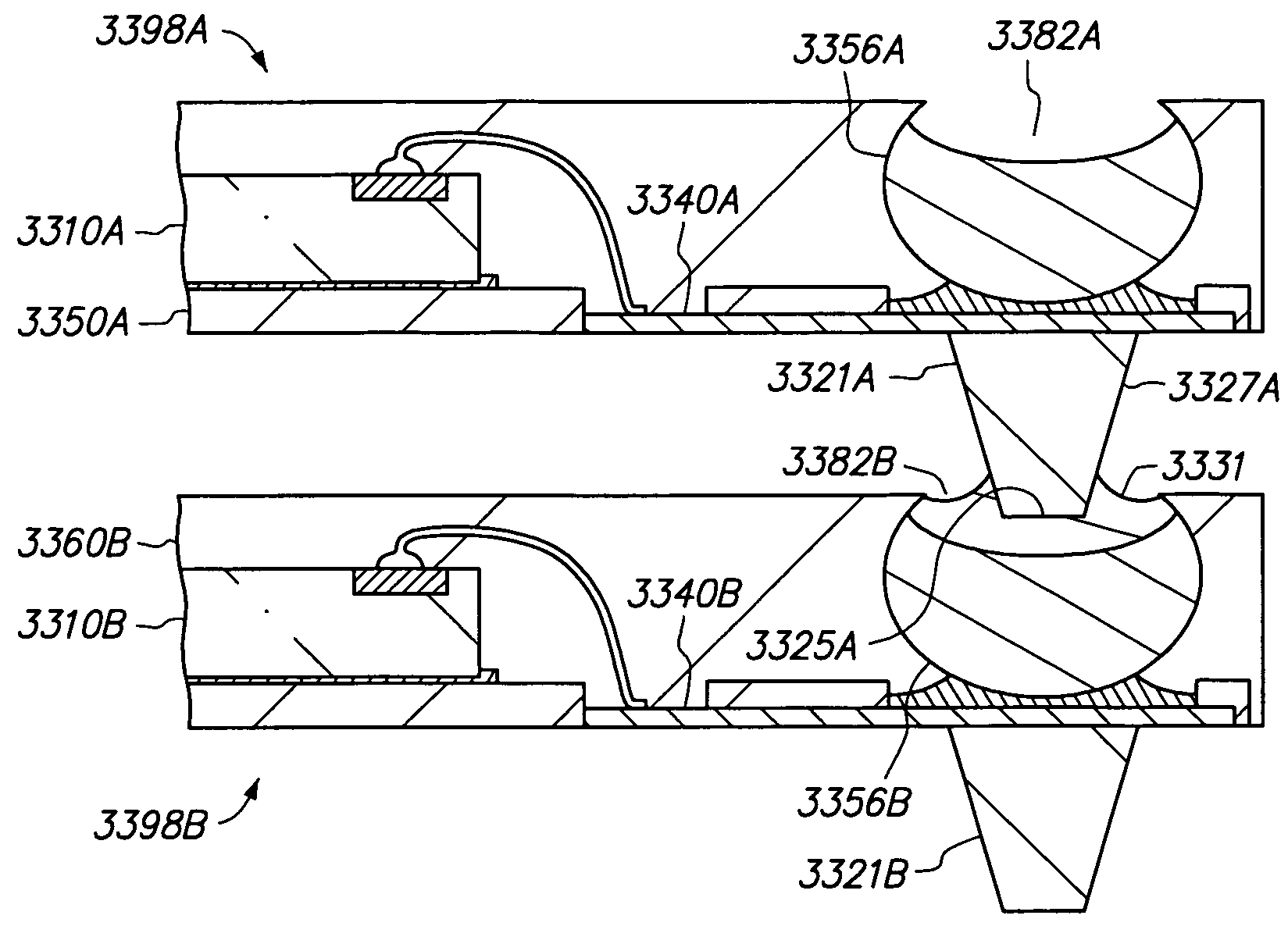
[0124]FIGS. 1A-26A, 1B-26B and 1C-26C are cross-sectional, top and bottom views, respectively, of a method of making a semiconductor chip assembly in accordance with a first embodiment of the present invention.

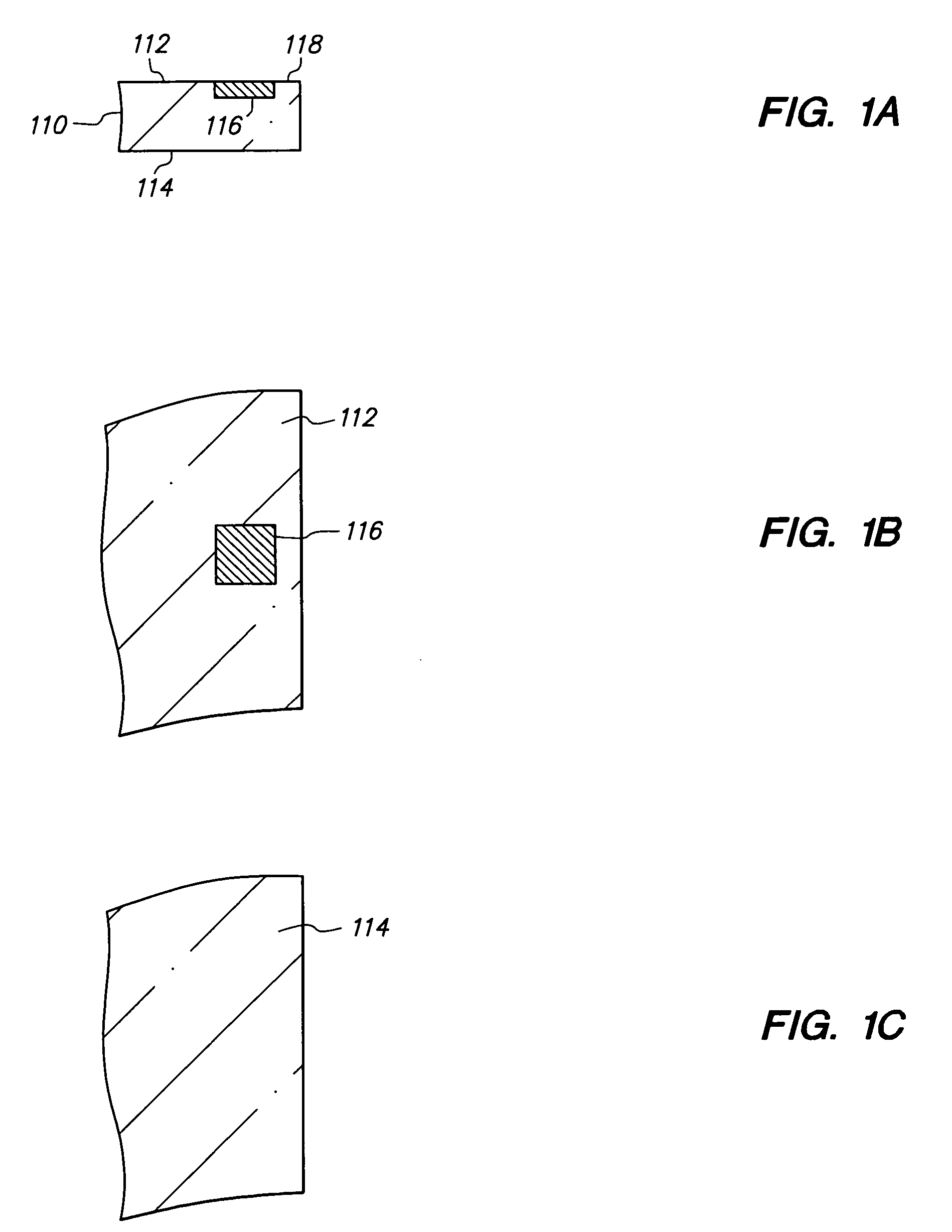
[0125]FIGS. 1A, 1B and 1C are cross-sectional, top and bottom views, respectively, of semiconductor chip 110 which is an integrated circuit in which various transistors, circuits, interconnect lines and the like are formed (not shown). Chip 110 includes opposing major surfaces 112 and 114 and has a thickness (between surfaces 112 and 114) of 150 microns. Surface 112 is the active surface and includes conductive pad 116 and passivation layer 118.

[0126]Pad 116 is substantially aligned with passivation layer 118 so that surface 112 is essentially flat. Alternatively, if desired, pad 116 can extend above or be recessed below passivation layer 118. Pad 116 provides a bonding site to electrically couple chip 110 with external circuitry. Thus, pad 116 can be an input / output pad or a ...


PUM


Abstract

A method of making a three-dimensional stacked semiconductor package includes providing a first semiconductor chip assembly that includes a first chip, a first conductive trace and a first encapsulant, wherein the first conductive trace includes a first metal pillar, providing a second semiconductor chip assembly that includes a second chip, a second conductive trace and a second encapsulant, wherein the second encapsulant includes a second aperture, and then positioning the first and second assemblies such that the first assembly overlaps the second assembly and the first metal pillar extends into the second aperture.

Description

CROSS-REFERENCE TO RELATED APPLICATIONS[0001]This application is a continuation of U.S. application Ser. No. 10 / 971,856 filed Oct. 22, 2004, now U.S. Pat. No. 7,129,113, which is a continuation of U.S. application Ser. No. 10 / 966,816 filed Oct. 15, 2004, now U.S. Pat. No. 7,067,911, which is a continuation-in-part of U.S. application Ser. No. 10 / 922,280 filed Aug. 19, 2004, now U.S. Pat. No. 7,009,297, which is a continuation-in-part of U.S. application Ser. No. 10 / 307,218 filed Nov. 29, 2002, now U.S. Pat. No. 6,809,414, which is a divisional of U.S. application Ser. No. 09 / 997,973 filed Nov. 29, 2001, now U.S. Pat. No. 6,492,252, which is a continuation-in-part of U.S. application Ser. No. 09 / 917,339 filed Jul. 27, 2001, now U.S. Pat. No. 6,537,851, which is a continuation-in-part of U.S. application Ser. No. 09 / 878,626 filed Jun. 11, 2001, now U.S. Pat. No. 6,653,217, which is a continuation-in-part of U.S. application Ser. No. 09 / 687,619 filed Oct. 13, 2000, now U.S. Pat. No. 6,...

Claims


Application Information

Patent Timeline
IPC IPC(8): H01L21/44
CPCH01L21/6835H01L23/3128H01L23/49517H01L24/16H01L24/24H01L24/48H01L25/0657H01L25/105H01L2924/014H01L2924/078H01L2924/09701H01L2924/14H01L2924/15311H01L2924/15331H01L2924/19041H01L2924/19043H01L2924/3025H01L24/29H01L24/45H01L2221/68345H01L2224/13099H01L2224/16H01L2224/18H01L2224/45144H01L2224/48091H01L2224/48227H01L2224/4824H01L2224/48465H01L2224/48599H01L2224/73204H01L2224/73215H01L2224/73217H01L2224/73265H01L2224/76155H01L2224/92144H01L2225/0651H01L2225/06541H01L2225/06586H01L2924/01011H01L2924/01012H01L2924/01013H01L2924/01014H01L2924/01015H01L2924/01022H01L2924/01027H01L2924/01028H01L2924/01029H01L2924/0103H01L2924/0104H01L2924/01046H01L2924/01047H01L2924/0105H01L2924/01074H01L2924/01077H01L2924/01078H01L2924/01079H01L2924/01082H01L2924/01083H01L2924/01327H01L2224/32145H01L2224/32225H01L2924/01005H01L2924/01006H01L2924/01019H01L2924/01024H01L2924/01033H01L2924/1815H01L2224/45147H01L2225/1023H01L2225/1035H01L2225/1058H01L2225/1094H01L2924/10253H01L2224/82102H01L2924/00014H01L2924/00H01L2924/3512H01L2924/00012H01L2924/00011H01L2924/181H01L2224/85207H01L24/73H01L2224/05026H01L2224/05548H01L2224/05571H01L2224/05573H01L2224/05001H01L21/568H01L2924/18162H01L24/82H01L24/03
Inventor LIN, CHARLES W. C.CHIANG, CHENG-LIEN
Owner BRIDGE SEMICON
Features
  • Generate Ideas
  • Intellectual Property
  • Life Sciences
  • Materials
  • Tech Scout
  • Unparalleled Data Quality
  • Higher Quality Content
  • 60% Fewer Hallucinations
Learn More