Multi-mode crystal oscillator

a crystal oscillator and multi-mode technology, applied in the field of communication systems, can solve the problems of difficult design challenge to develop a wireless communication device, integrated circuit, wireless communication device engineers, etc., and achieve the effect of facilitating adjustment of operation

Inactive Publication Date: 2007-09-04
AVAGO TECH INT SALES PTE LTD
View PDF8 Cites 29 Cited by
  • Summary
  • Abstract
  • Description
  • Claims
  • Application Information

AI Technical Summary

Benefits of technology

[0012]In one embodiment of the present invention, two crystal oscillator circuits are coupled in parallel to provide differing performance according to mode. Generally, a first circuit provides low phase noise and high accuracy while a second circuit provides greater phase noise within an acceptable tolerance while consuming significantly less power in a low power mode of operation. The second circuit includes an separate amplifier for the low power operation that tolerates a relatively smaller input signal swing but that consumes even less power. The first circuit, which comprises selectable amplification elements, and the second circuit are coupled in parallel with selectable resistive elements and capacitive elements to provide varying amounts of amplification and filtering according to whether an operational mode is in startup mode, a normal mode, or a low power mode of operation.
[0015]As will be described in greater detail below, a crystal oscillator is coupled to the first amplifier having an adjustable amplification block. Accordingly, the gain level of the first amplifier may be adjusted according to desired operation. Similarly, across the input and output nodes, a plurality of parallel coupled resistors are coupled to provide adjustable resistance levels in conjunction with a plurality of parallel coupled capacitors that are also selectable and are coupled across the input and output nodes of the first and second amplifiers. Accordingly, the adjustable resistance block with selectable resistors, in addition to a pair of the adjustable capacitive blocks with selectable capacitors, facilitate adjustment of the operation of the multi-mode crystal oscillator. In the specific embodiments of the invention, MOSFET devices are used as switches to operatively couple or decouple the resistors and capacitors of the adjustable resistance block and the adjustable capacitive blocks.

Problems solved by technology

As the demand for enhanced performance (e.g., reduced interference and / or noise, improved quality of service, compliance with multiple standards, increased broadband applications, etc.), smaller sizes, lower power consumption, and reduced cost continue to be asserted, wireless communication device engineers are faced with a very difficult design challenge to develop a wireless communication device that satisfies requirements that sometimes appear to be mutually exclusive.
Integrated circuits, however, by their very nature, cannot incorporate an internal crystal oscillator.
Thus, most current designs include clock systems that consume sufficient power to provide accurate time keeping.
Known designs that reduce power consumption during a sleep mode often fail to provide the desired accuracy.

Method used


Image

  • Multi-mode crystal oscillator
  • Multi-mode crystal oscillator
  • Multi-mode crystal oscillator

Examples


Embodiment Construction

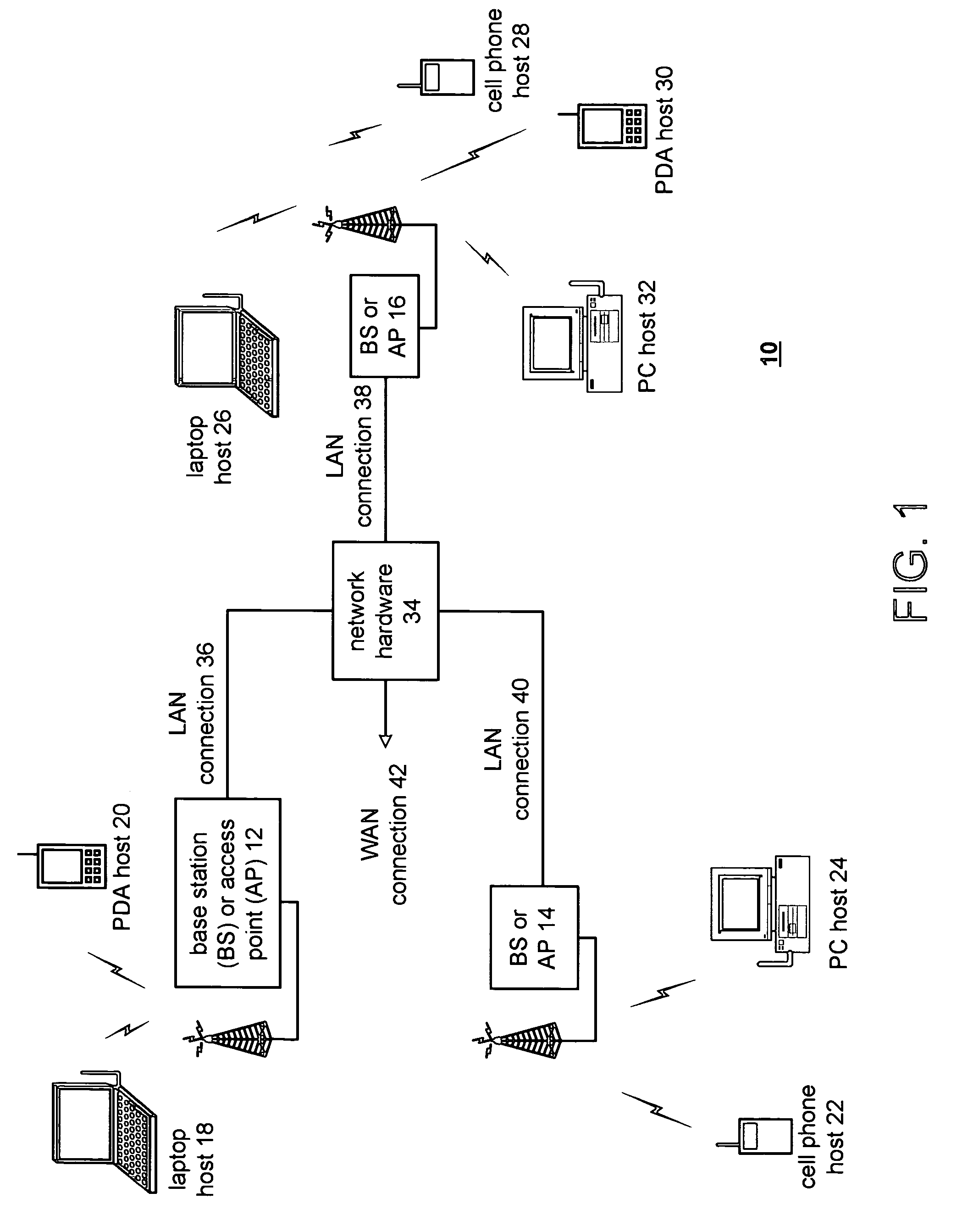
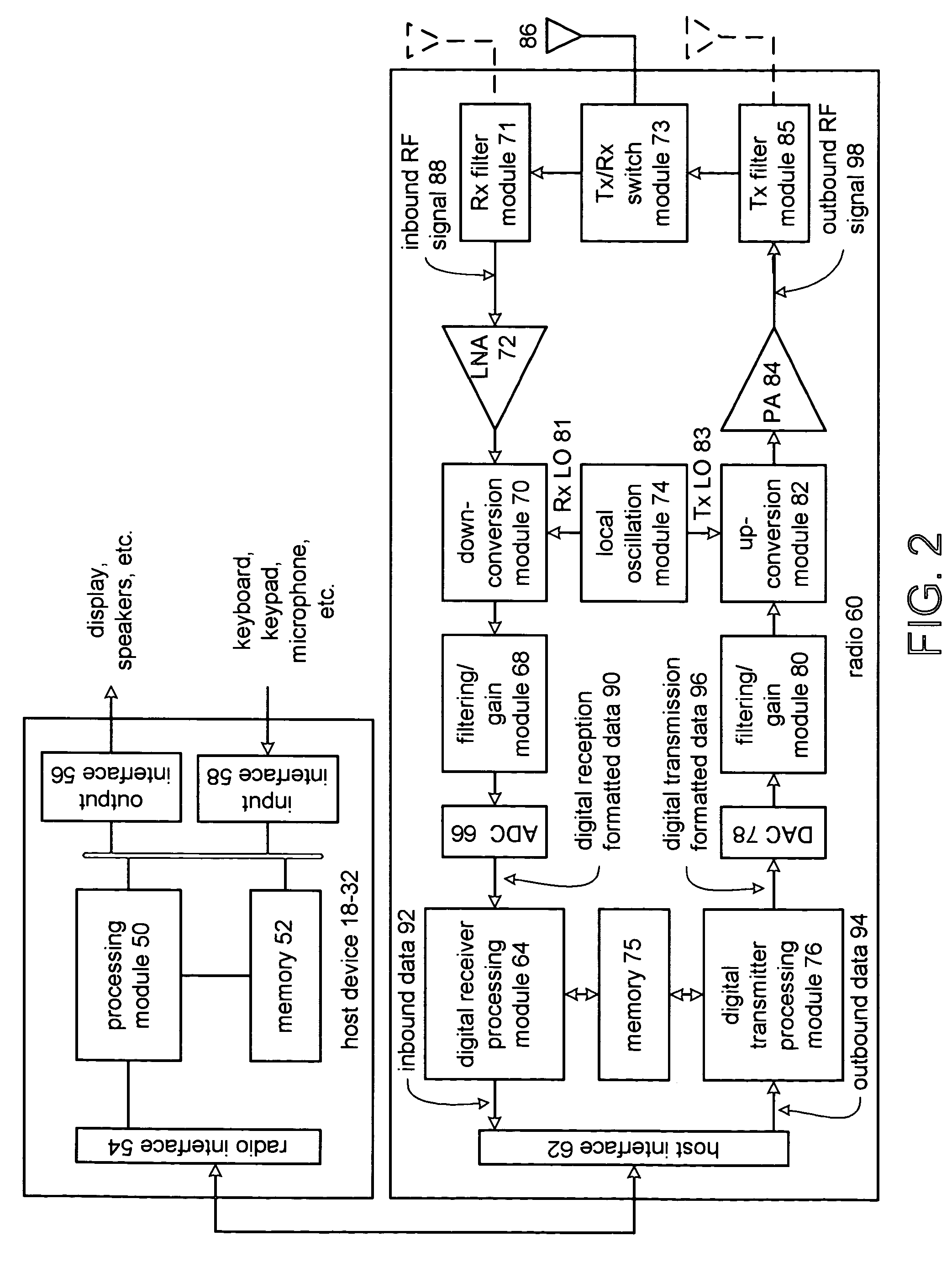
[0023]FIG. 1 is a schematic block diagram illustrating a communication system 10 that includes a plurality of base stations and access points 12-16, a plurality of wireless communication devices 18-32 and a network hardware component 34. Any one of the wireless communication devices may include an integrated temperature sensor formed according to an embodiment of the invention. The wireless plurality of communication devices 18-32 may be laptop host computers 18 and 26, personal digital assistant hosts 20 and 30, personal computer hosts 24 and 32 and / or cellular telephone hosts 22 and 28. The details of the wireless communication devices will be described in greater detail with reference to FIG. 2.

[0024]The base stations or access points 12-16 are operably coupled to the network hardware component 34 via local area network (LAN) connections 36, 38 and 40. The network hardware component 34, which may be a router, switch, bridge, modem, system controller, etc., provides a wide area ne...


PUM


Abstract

In one embodiment of the present invention, two crystal oscillator circuits are coupled in parallel to provide differing performance according to mode. Generally, a first circuit provides low phase noise and high accuracy while a second circuit provides greater phase noise within an acceptable tolerance while consuming significantly less power in a low power mode of operation. The second circuit includes an entirely separate amplifier for the low power operation that tolerates a relatively smaller input signal swing but that consumes even less power. The first circuit, which comprises selectable amplification elements, and the second circuit are coupled in parallel with selectable resistive elements and capacitive elements to provide varying amounts of amplification and filtering according to whether an operational mode is in a startup mode, a normal mode, or a low power mode of operation.

Description

BACKGROUND[0001]1. Technical Field[0002]This invention relates generally to communication systems and, more particularly, to integrated time references within a device for use either as a clock reference or calibration master within portable electronics including radio frequency (RF) wireless devices operating in wireless communication systems.[0003]2. Related Art[0004]Communication systems are known to support wireless and wire lined communications between wireless and / or wired communication devices. Such communication systems range from national and / or international cellular telephone systems to the Internet to point-to-point in-home wireless networks. Each type of communication system is constructed, and hence operates, in accordance with one or more communication standards. For instance, wireless communication systems may operate in accordance with one or more standards including, but not limited to, IEEE 802.11, Bluetooth, advanced mobile phone services (AMPS), digital AMPS, gl...

Claims


Application Information

Patent Timeline
Patent Type & Authority Patents(United States)
IPC IPC(8): H04B1/04H04B1/16
CPCG06F1/3203G06F1/324H03B5/06H03B5/366H03K3/0307H03K3/3545H04W52/029H03B2200/0046H03B2200/005H03B2200/0052H03B2200/0094Y02B60/1217Y02B60/50Y02D10/00Y02D30/70
Inventor KAPPES, MICHAEL
Owner AVAGO TECH INT SALES PTE LTD
Why Eureka
Try Eureka