Method of checking optical proximity correction data

a technology of optical proximity correction and data verification, applied in the field of electronic design automation (eda) software, can solve the problems that conventional design rules and optical proximity correction (opc) cannot adequately manage the new challenges, and the chip fabrication process becomes so complex, so as to facilitate systematic correction and prevention of defects in integrated circuit layout design, improve the accuracy and performance and speed up the process of optical proximity correction data verification.

Active Publication Date: 2007-09-25
ANCHOR SEMICON
View PDF29 Cites 42 Cited by
  • Summary
  • Abstract
  • Description
  • Claims
  • Application Information

AI Technical Summary

Benefits of technology

[0009]The invention is a method of inspecting integrated circuit (IC) full-chip layout data to locate layout pattern induced defects and weak points that cause functional failure or performance degradation for integrated circuits manufactures in subwavelength technology. The embodiment of the invention is a computer program that contains at least the following innovations. Starting from pre-OPC layout data, the program refers to available post-OPC layout data or generates post-OPC data condition to do the inspection based on the mode

Problems solved by technology

As technology advances to 0.18 microns and smaller, integrated circuit feature size becomes smaller than photolithography wavelength, chip fabrication process becomes so complex that conventional design rules

Method used


Image

  • Method of checking optical proximity correction data
  • Method of checking optical proximity correction data
  • Method of checking optical proximity correction data

Examples


Embodiment Construction

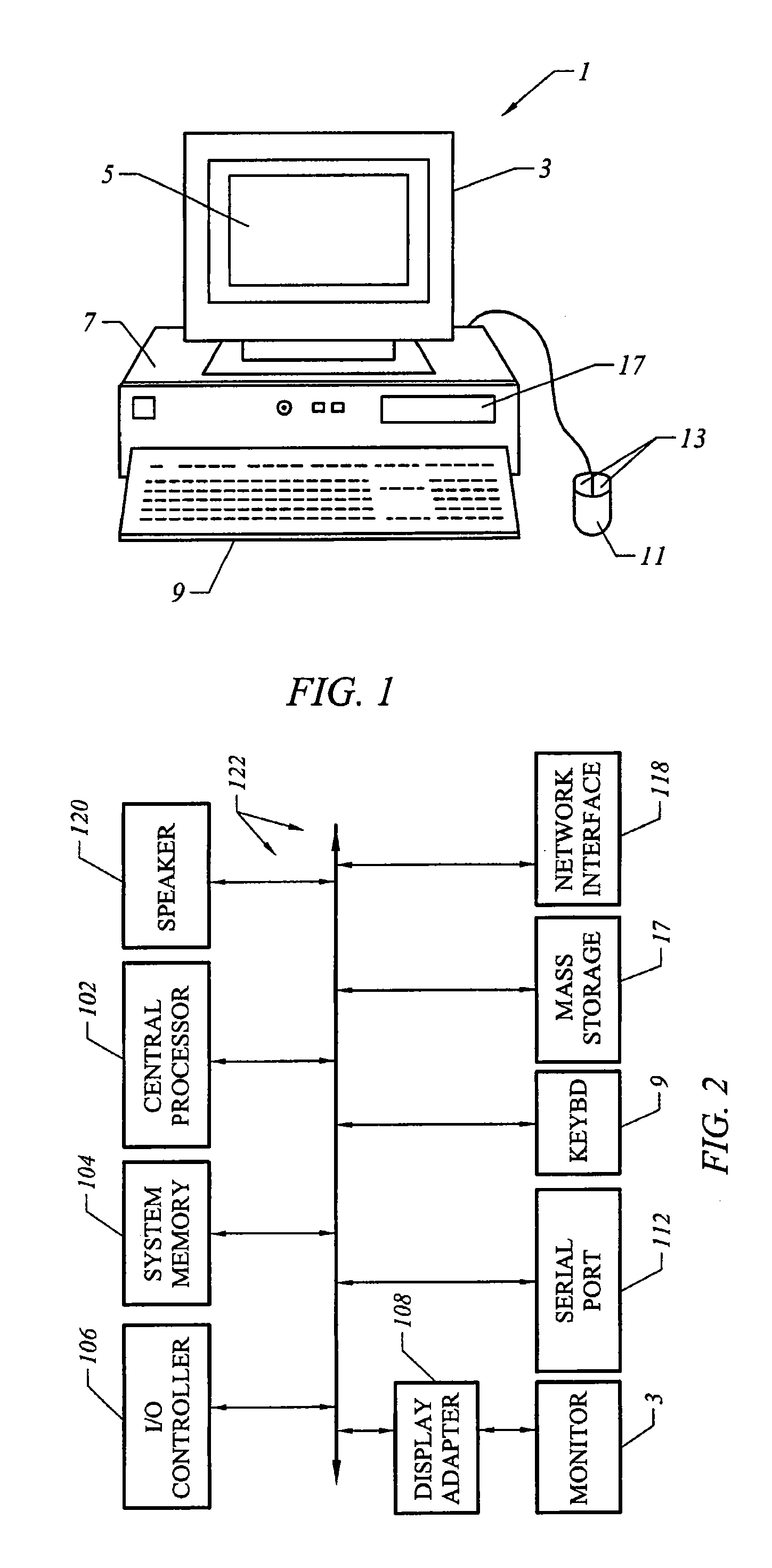
[0039]FIG. 1 shows a system of the present invention for estimating the performance of an integrated circuit. FIG. 1 may comprise a computer or digital system used to execute the software of the present invention. For example, the method of the present invention may be performed using a computer workstation. FIG. 1 shows a computer system 1 that includes a monitor 3, screen 5, cabinet 7, keyboard 9, and mouse 11. Mouse 11 may have one or more buttons such as mouse buttons 13. Cabinet 7 houses familiar computer components, some of which are not shown, such as a processor, memory, mass storage devices 17, and the like. Mass storage devices 17 may include mass disk drives, floppy disks, Iomega® ZIP™ disks, magnetic disks, fixed disks, hard disks, Flash disks and storage, CD-ROMs, recordable CDs, DVDs, tape storage, reader, and other similar media, and combinations of these. A binary, machine-executable version, of the software of the present invention may be stored or reside on mass st...


PUM


Abstract

A method of inspecting full-chip mask data to locate layout pattern design induced defects and weak points that cause functional failure or performance degradation for integrated circuits (ICs) manufactured in subwavelength technology. Given the pre-OPC integrated circuit design layout data, the method of present invention refers to available post-OPC data or generates post-OPC data condition to do the inspection based on the modeling of integrated circuit wafer patterning. Build-in direct checks of specified electrical functional defects and a multilayer pattern-centric approach are used to improve the accuracy and performance. A technique of adaptive search is used to speed up the critical dimension search during the process of optical proximity correction data verification. A defect synthesis capability is supplied for defect disposition to facilitate systematic correction and prevention of the defects in integrated circuit layout design.

Description

[0001]This application claims the benefit of U.S. provisional patent application 60 / 498,424, filed Aug. 27, 2003, which is incorporated by reference.BACKGROUND OF THE INVENTION[0002]The present invention relates to the field of electronic design automation (EDA) software, and more specifically, to techniques of checking and verifying the quality of optical proximity correction (OPC) data for an integrated circuit design.[0003]Integrated circuit technology is a marvel of the modem age. Integrated circuits are used in many applications such as computers, consumer electronics, networking, and telecommunications. There are many types of integrated circuits including microprocessors, microcontrollers, application specific integrated circuits (ASICs), gate arrays, programmable logic devices (PLDs), field programmable gate arrays (FPGAs), dynamic random access memories (DRAMs), static random access memories (SRAMs), erasable programmable read only memories (EPROMs), electrically erasable p...

Claims


Application Information

Patent Timeline
IPC IPC(8): G06F17/50
CPCG03F1/36G03F1/84
Inventor YING, CHANGSHENG
Owner ANCHOR SEMICON
Why Eureka
Try Eureka