Semiconductor device having a pixel matrix circuit that includes a pixel TFT and a storage capacitor

a semiconductor device and circuit technology, applied in the field of semiconductor devices, can solve the problems of large current (current flowing when the tft is in an off state) and is not suitable for a circuit, and achieve the effect of enhancing the reliability of a semiconductor device (electronic equipment) and high reliability

Inactive Publication Date: 2007-10-02
SEMICON ENERGY LAB CO LTD
View PDF98 Cites 39 Cited by
  • Summary
  • Abstract
  • Description
  • Claims
  • Application Information

AI Technical Summary

Benefits of technology

[0011]An object of the present invention is to provide an AM-LCD having high reliability by constructing circuits of the AM-LCD from TFTs having different structures to suit the respective functions of the circuits. The invention aims to accordingly enhance the reliability of a semiconductor device (electronic equipment) having this AM-LCD.
[0012]Another object of the present invention is to provide a TFT structure for reducing OFF current as much as possible and a structure for improving a capacity of a storage capacitance (also called an auxiliary capacitor) for a pixel matrix circuit of an AM-LCD.
[0026]It is effective to improve the aperture ratio by forming the storage capacitor from the high dielectric constant film under a source wiring line of the pixel matrix circuit, and / or under a gate wiring line thereof.

Problems solved by technology

However, the TFT is considered as not so equal in terms of reliability to a MOSFET that is formed on a single crystal semiconductor substrate.
One of causes of the phenomena is characteristic degradation due to hot carriers that accompany enlargement of a channel electric field.
However, application of the GOLD structure (in this specification, a structure having an LDD region to which a gate voltage is applied is called a GOLD structure whereas a structure having merely an LDD region to which a gate voltage is not applied is called an LDD structure) to a TFT has a problem of OFF current (current flowing when the TFT is in an OFF state) being larger than in the LDD structure.
For that reason, the GOLD structure is not suitable for a circuit in which OFF current should be as small as possible, such as a pixel matrix circuit of an AM-LCD.

Method used


Image

  • Semiconductor device having a pixel matrix circuit that includes a pixel TFT and a storage capacitor
  • Semiconductor device having a pixel matrix circuit that includes a pixel TFT and a storage capacitor
  • Semiconductor device having a pixel matrix circuit that includes a pixel TFT and a storage capacitor

Examples


embodiment 1

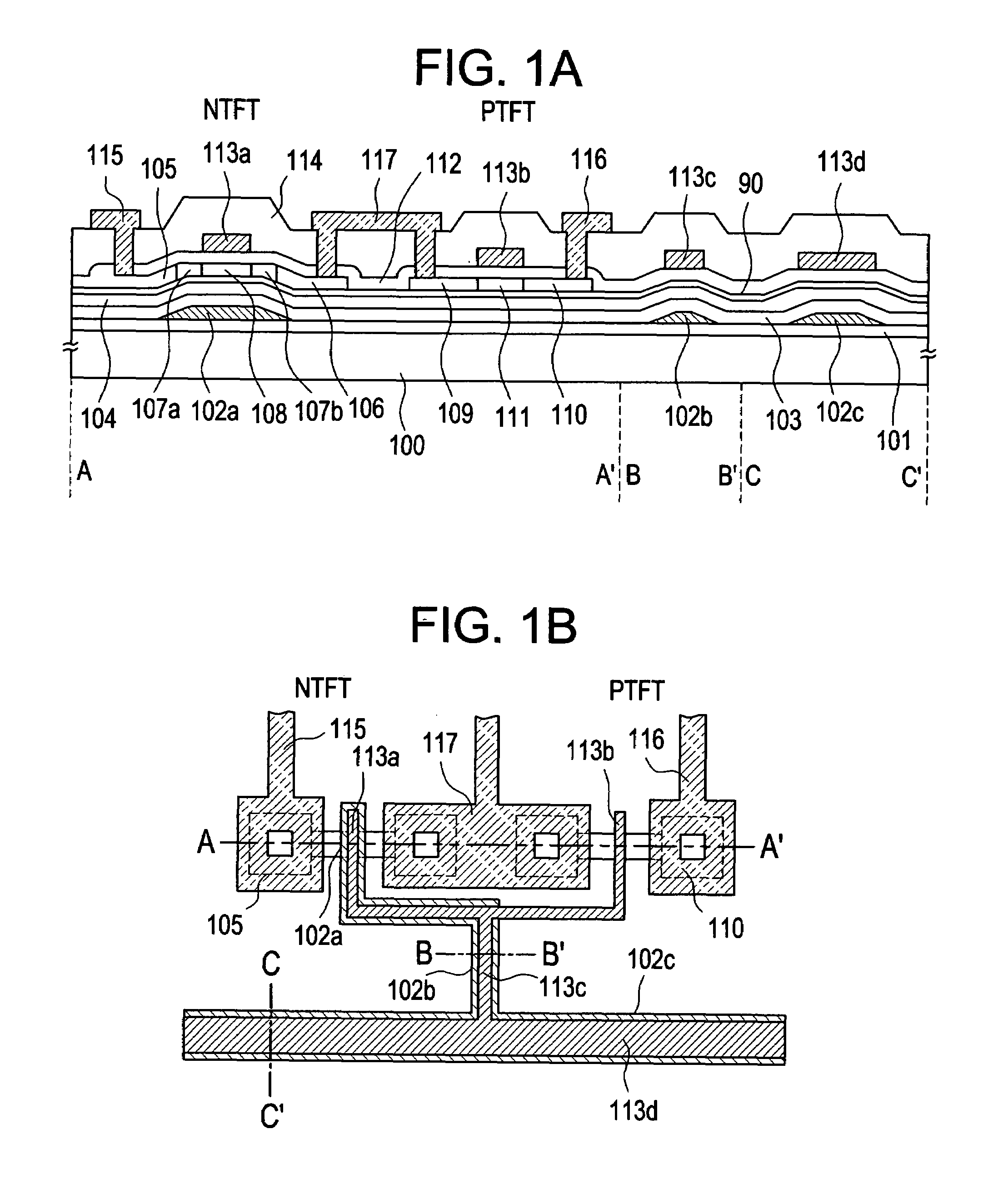
[0097]In this embodiment, a method of manufacturing the CMOS circuit described in Embodiment Mode 1 will be described. The description will be given with reference to FIG. 3.

[0098]First, a glass substrate is prepared as a substrate 300. A silicon oxide film with a thickness of 200 nm is formed thereon by sputtering as a base film 301. On the base film, first wiring lines 302a, 302b, and 302c are formed. The material of the first wiring lines is a tantalum film formed by sputtering. An oxide film may be formed on a surface of the tantalum film.

[0099]Other metal films, alloy films, or a laminate of those may of course be used because the first wiring lines 302a, 302b, and 302c can be formed of any film as long as it has conductivity. A film that can be formed by patterning with a small taper angle is effective in improving the levelness.

[0100]Next, a tantalum oxide film is formed again by sputtering. In this embodiment, the thickness thereof is set to 10 to 500 nm (desirably 50 to 300...

embodiment 2

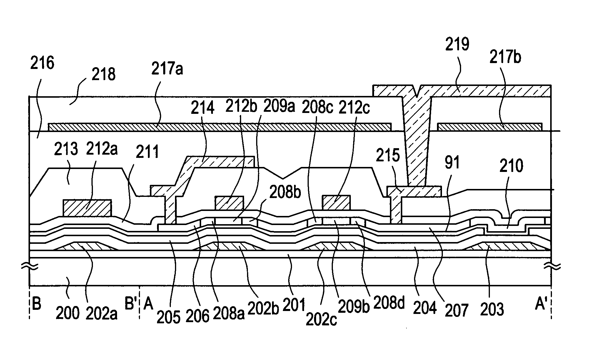
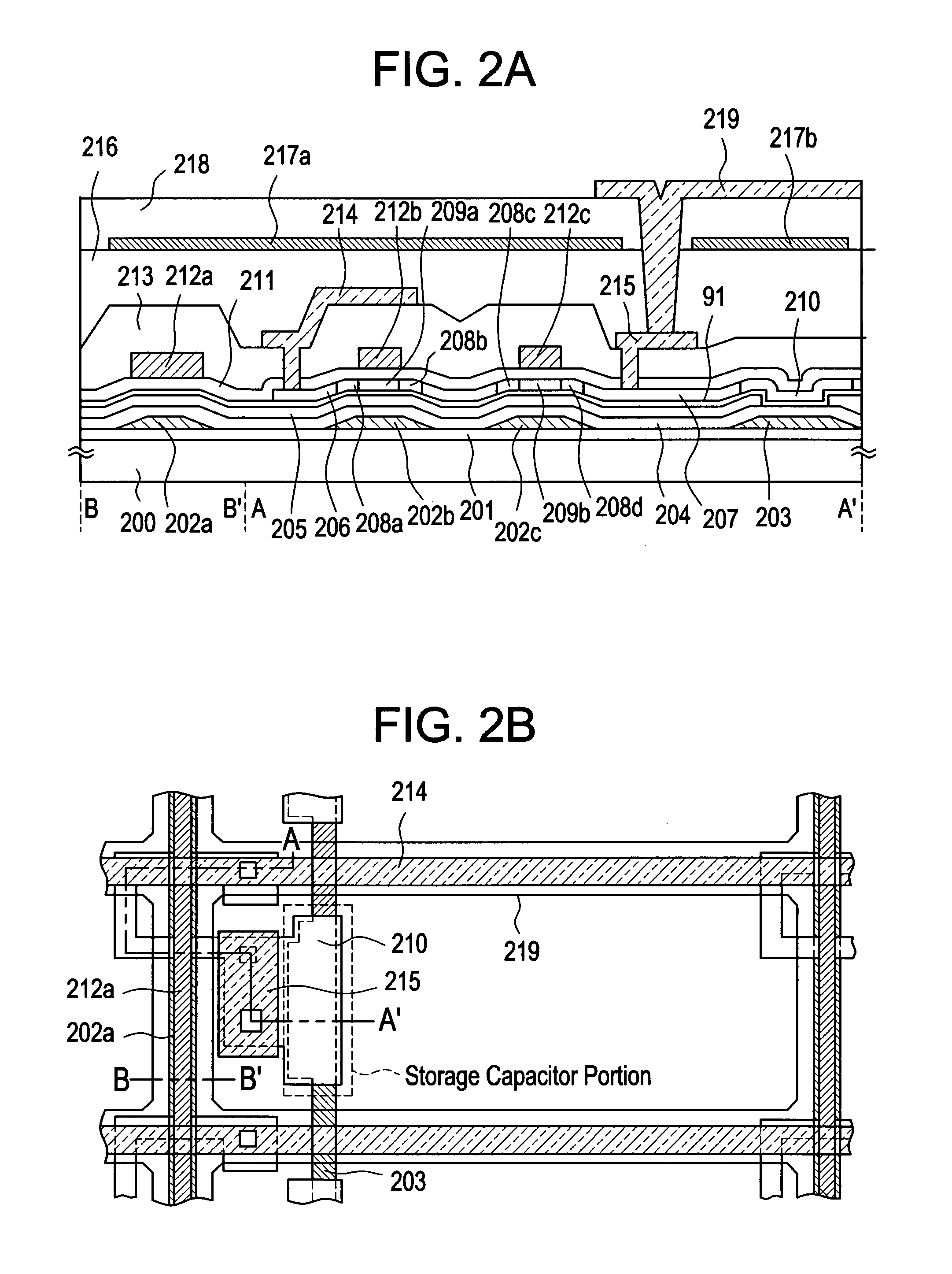
[0130]In this embodiment, a method of manufacturing the pixel matrix circuit described in Embodiment Mode 2 will be described. The description will be given with reference to FIGS. 4 and 5. The pixel matrix circuit is formed on the same substrate as the CMOS circuit shown in Embodiment 1 at the same time. Therefore, the description will be given in relation to the manufacturing process of Embodiment 1 and the symbols identical with those in FIG. 3 are used when necessary.

[0131]First, the base film 301 is formed on the glass substrate 300 from a tantalum oxide film. On the base film, first wiring lines 401a, 401b, and 401c and a capacitor wiring line 402 are formed. The first wiring line 401a corresponds to the first wiring line 202a in FIG. 2A, the first wiring line 401b corresponds to the first wiring line 202b in FIG. 2A, and the first wiring line 401c corresponds to the first wiring line 202c in FIG. 2A.

[0132]The capacitor wiring line 402 corresponds to the capacitor wiring line ...

embodiment 3

[0157]In this embodiment, an AM-LCD is provided with a pixel matrix circuit and a CMOS circuit (a driver circuit and a signal processing circuit constructed of CMOS circuits, to be exact) according to the present invention, and the appearance thereof is shown in FIG. 6.

[0158]On an active matrix substrate 601, a pixel matrix circuit 602, a signal line driving circuit (source driver circuit) 603, scanning line driving circuits (gate driver circuits) 604, and a signal processing circuit (including a signal dividing circuit, a D / A converter circuit, and a γ correction circuit) 605 are formed. An FPC (flexible printed circuit) 606 is attached to the active matrix substrate. Denoted by 607 is an opposite substrate.

[0159]The various circuits formed on the active matrix substrate 601 are illustrated in detail in a block-diagram of FIG. 7.

[0160]In FIG. 7, 701 denotes a pixel matrix circuit that functions as an image display unit. 702a, 702b, and 702c represent a shift register circuit, a lev...


PUM

PropertyMeasurementUnit
dielectric constantaaaaaaaaaa
electric potentialaaaaaaaaaa

Abstract

In a CMOS circuit formed on a substrate 100, a subordinate gate wiring line (a first wiring line) 102a and main gate wiring line (a second wiring line) 113a are provided in an n-channel TFT. The LDD regions 107a and 107b overlap the first wiring line 102a and not overlap the second wiring line 113a. Thus, applying a gate voltage to the first wiring line forms the GOLD structure, while not applying forms the LLD structure. In this way, the GOLD structure and the LLD structure can be used appropriately in accordance with the respective specifications required for the circuits.

Description

BACKGROUND OF THE INVENTION[0001]1. Field of the Invention[0002]The present invention relates to a semiconductor device having a circuit composed of a thin film transistor (hereinafter referred to as TFT). For example, the invention relates to an electro-optical device represented by a liquid crystal display panel and to electronic equipment mounted with the electro-optical device as a component.[0003]In this specification, a ‘semiconductor device’ refers to a device in general that utilizes semiconductor characteristics to function, and electro-optical devices, semiconductor circuits, and electronic equipment are semiconductor devices.[0004]2. Description of Related Art[0005]A thin film transistor (hereinafter referred to as TFT) can be formed on a transparent glass substrate, and hence its application to an active matrix liquid crystal display (hereinafter referred to as AM-LCD) has been developed actively. A TFT utilizing a crystalline semiconductor film (typically, a polysilicon...

Claims


Application Information

Patent Timeline
Patent Type & Authority Patents(United States)
IPC IPC(8): H01L29/06H01L29/08H01L29/786G02B27/01G02F1/136G02F1/1368H01L21/336H01L21/77H01L21/84H01L27/12H01L27/13
CPCG02B27/017H01L27/1255H01L29/78648H01L29/78645
Inventor YAMAZAKI, SHUNPEIYAMAZAKI, YUKOYAMA, JUNIKEDA, TAKAYUKISHIBATA, HIROSHIKITAKADO, HIDEHITOFUKUNAGA, TAKESHI
Owner SEMICON ENERGY LAB CO LTD
Why Eureka
Try Eureka