

High speed data access memory arrays
a memory array and high-speed technology, applied in the field of memory arrays, can solve the problems of resistive and capacitive (rc) delays on the global bit line becoming a problem, and the length of the wire becoming too long, and achieve the effect of reducing rc delays
- Summary
- Abstract
- Description
- Claims
- Application Information
AI Technical Summary
Benefits of technology
Problems solved by technology
Method used
Image

Examples
Embodiment Construction
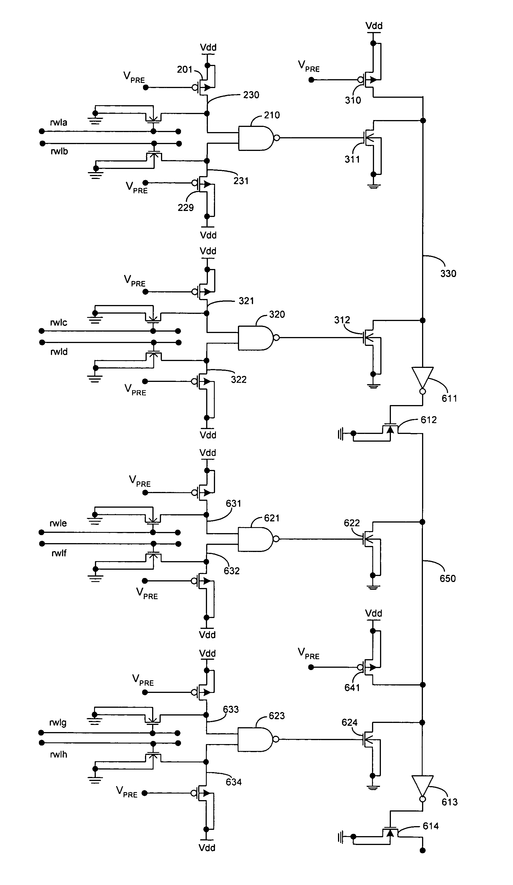
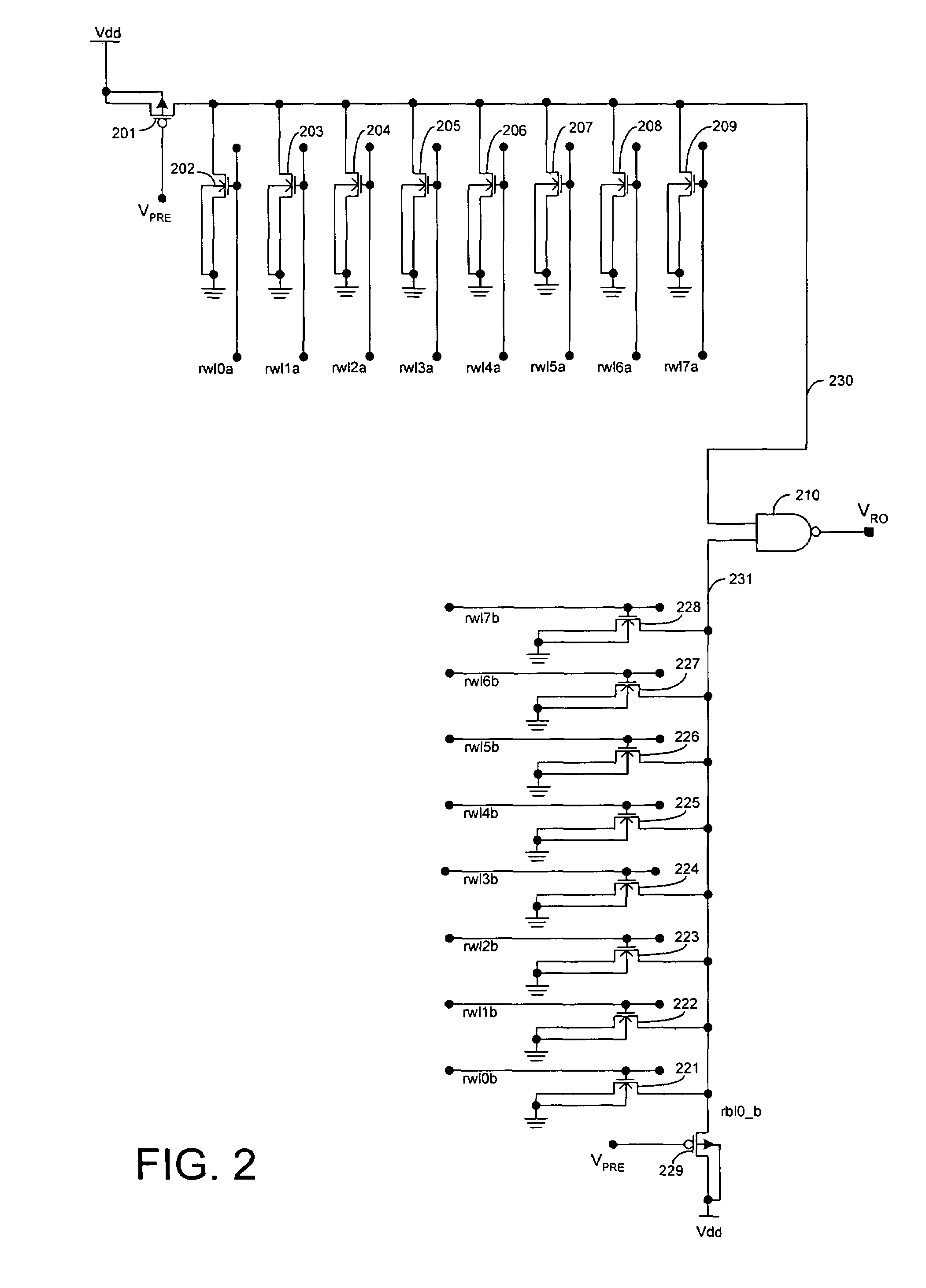
[0024]The present invention provides high speed techniques for reading data bits from memory arrays. Memory arrays comprise numerous memory cells that are usually arranged in rows and columns. Memory arrays of the present invention can comprise SRAM cells, dynamic random access memory (DRAM) cells, read only memory (ROM) cells, electrically erasable programmable read only memory (EEPROM) cells, EPROM cells, programmable logic arrays (PLAs), FLASH memory, and many other types of memory cells.
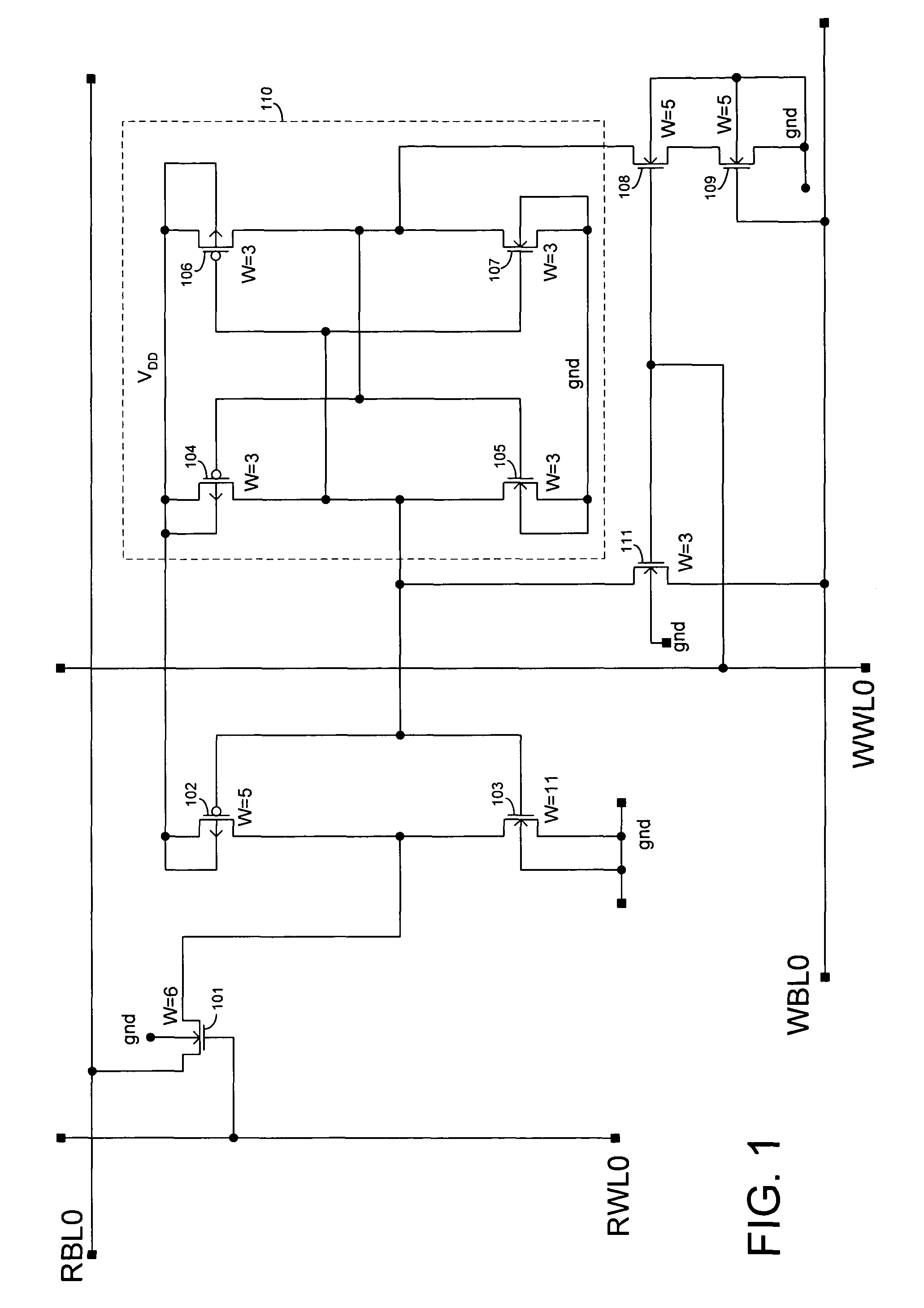
[0025]An example of a multi-port SRAM cell that can be used in a memory array of the present invention is illustrated in FIG. 1. The SRAM cell 110 of FIG. 1 includes two cross coupled inverters coupled between supply voltage VDD and ground. The first inverter includes p-channel transistor 104 and n-channel transistor 105. The second inverter includes p-channel transistor 106 and n-channel transistor 107.
[0026]SRAM cell 110 is controlled by the write word line WWL0. When the signal on write word l...
PUM
 Abstract
Description
Claims
Application Information