Methods and apparatus for making integrated-circuit wiring from copper, silver, gold, and other metals

a technology of integrated circuit wiring and copper, applied in the direction of instruments, vacuum evaporation coatings, coatings, etc., can solve the problems of reducing the production efficiency of integrated circuits. , to achieve the effect of reducing defects, facilitating the formation of copper diffusion barriers, and promoting fabrication efficiency

Inactive Publication Date: 2007-10-23
ROUND ROCK RES LLC
View PDF254 Cites 29 Cited by
  • Summary
  • Abstract
  • Description
  • Claims
  • Application Information

AI Technical Summary

Benefits of technology

[0009]To address these and other needs, the inventors devised unique wafer-processing chambers and methods of forming barrier and seed layers. One embodiment of the wafer-processing chamber includes equipment for physical vapor deposition and equipment for chemical vapor deposition, two processes which facilitate formation of copper-diffusion barriers an...

Problems solved by technology

The first is that typical copper-diffusion barriers add appreciable resistance to the copper wiring, and thus negate some of the advantages of using copper.
However, moving wafers from...

Method used


Image

  • Methods and apparatus for making integrated-circuit wiring from copper, silver, gold, and other metals
  • Methods and apparatus for making integrated-circuit wiring from copper, silver, gold, and other metals
  • Methods and apparatus for making integrated-circuit wiring from copper, silver, gold, and other metals

Examples


Embodiment Construction

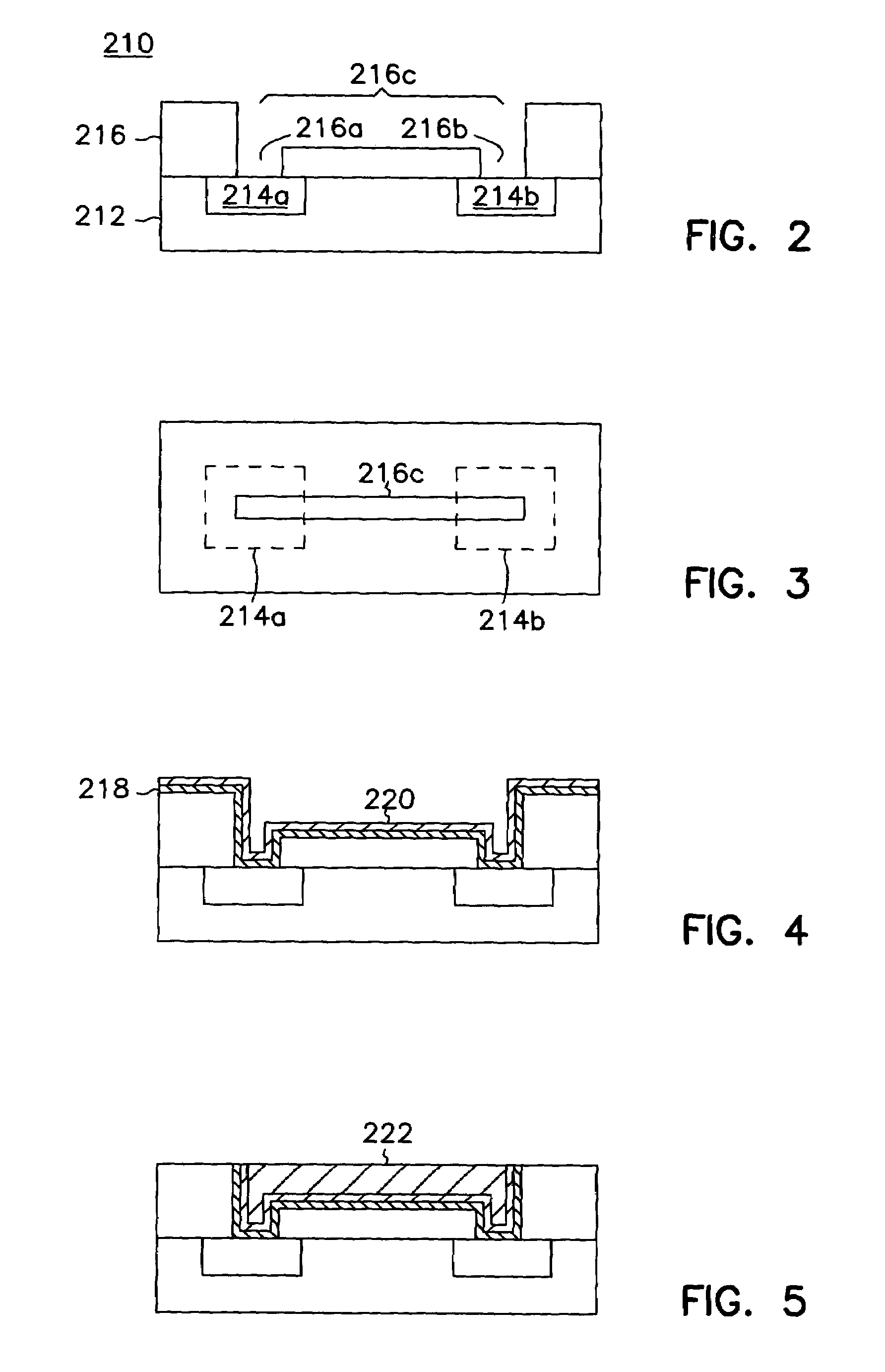
[0016]The following detailed description, which references and incorporates FIGS. 1-6, describes and illustrates specific embodiments of the invention. These embodiments, offered not to limit but only to exemplify and teach the concepts of the invention, are shown and described in sufficient detail to enable those skilled in the art to implement or practice the invention. Thus, where appropriate to avoid obscuring the invention, the description may omit certain information known to those of skill in the art.

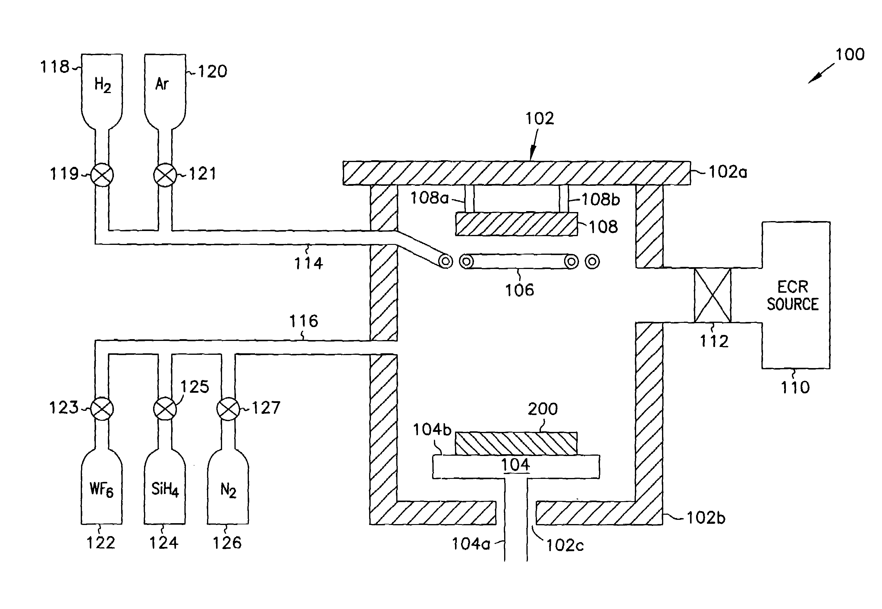
[0017]FIG. 1 shows an exemplary wafer-processing apparatus or system 100 which incorporates teachings of the present invention. In particular, system 100 includes a chamber 102, a wafer holder 104, an RF-gas-emission coil 106, a sputter target 108, an electron-cylotron-resonance (ECR) source 110, an isolation valve 112, gas inlets 114 and 116, gas (or more generally fluid) sources 118, 120, 122, 124, and 126, and mass-flow controllers 119, 121, 123, 125, and 127.

[0018]More partic...


PUM

PropertyMeasurementUnit
Lengthaaaaaaaaaa
Electrical conductivityaaaaaaaaaa
Compositionaaaaaaaaaa

Abstract

In recent years, copper wiring has emerged as a promising substitute for the aluminum wiring in integrated circuits, because copper offers lower electrical resistance and better reliability at smaller dimensions than aluminum. However, use of copper typically requires forming a diffusion barrier to prevent contamination of other parts of an integrated circuit and forming a seed layer to facilitate copper plating steps. Unfortunately, conventional methods of forming the diffusion barriers and seed layers require use of separate wafer-processing chambers, giving rise to transport delays and the introduction of defect-causing particles. Accordingly, the inventors devised unique wafer-processing chambers and methods of forming barrier and seed layers. One embodiment of the wafer-processing chamber includes equipment for physical vapor deposition and equipment for chemical vapor deposition to facilitate formation of diffusion barriers and seed layers within one chamber, thereby promoting fabrication efficiency and reducing defects.

Description

CROSS-REFERENCE TO RELATED APPLICATION(S)[0001]This patent application is a continuation of U.S. application Ser. No. 10 / 211,855, filed on Aug. 1, 2002, now issued as U.S. Pat. No. 6,756,298; which is a division of U.S. application Ser. No. 09 / 488,098, filed on Jan. 18, 2000, now issued as U.S. Pat. No. 6,429,120; the specifications of which are hereby incorporated by reference.TECHNICAL FIELD[0002]The present invention concerns methods of semiconductor device or integrated circuit manufacturing, particularly methods of forming interconnects from copper and other metals.BACKGROUND OF THE INVENTION[0003]Integrated circuits, the key components in thousands of electronic and computer products, are interconnected networks of electrical components fabricated on a common foundation, or substrate. Fabricators typically use various techniques, such as layering, doping, masking, and etching, to build thousands and even millions of microscopic resistors, transistors, and other electrical comp...

Claims


Application Information

Patent Timeline
IPC IPC(8): C23C14/34C23C16/00G02F1/1362H01L21/768H01L29/786
CPCC23C14/3471C23C16/517H01J37/3408H01L29/78696H01L21/76846H01L21/76856H01L21/76873H01L21/76843G02F1/13454
Inventor AHN, KIE Y.FORBES, LEONARD
Owner ROUND ROCK RES LLC
Why Eureka
Try Eureka