Micro-package, multi-stack micro-package, and manufacturing method therefor

a manufacturing method and micro-package technology, applied in the direction of electrical equipment, semiconductor devices, semiconductor/solid-state device details, etc., can solve the problems of reducing the efficiency of wire bonding, reducing the productivity and cost of wire bonding, and increasing parasitic capacitance and insertion loss, so as to improve the hermetical sealing of the package and prevent damage to the device inside the package

Active Publication Date: 2007-10-23
SAMSUNG ELECTRONICS CO LTD
View PDF3 Cites 57 Cited by
  • Summary
  • Abstract
  • Description
  • Claims
  • Application Information

AI Technical Summary

Benefits of technology

[0011]The present invention has been developed in order to address the above drawbacks and other problems associated with the conventional arrangement. An aspect of the present invention is to provide a micro package, a multi-stack micro package, and a manufacturing method therefor capable of improving hermetical sealing of the package at the same time of preventing damages to devices inside a package by using a low-temperature process upon wafer bonding.
[0017]Preferably, but not necessarily, the layer protects the device inside the micro package and prevents moisture absorption from outside.
[0030]Preferably, but not necessarily, the layer protects the device inside the micro package and prevents moisture absorption from outside.

Problems solved by technology

However, the micro gap wafer-level package disclosed in the U.S. Pat. No. 6,376,280 has a problem of increasing parasitic capacitance and insertion loss due to wire bonding.
Further, there exist problems of limitation on chip size reduction due to formation of the pads and damages to the inside of a package due to a process temperature increased over 350° C. Further, there exist problems of lowering productivity and cost increase due to the wire bonding.

Method used


Image

  • Micro-package, multi-stack micro-package, and manufacturing method therefor
  • Micro-package, multi-stack micro-package, and manufacturing method therefor
  • Micro-package, multi-stack micro-package, and manufacturing method therefor

Examples


Embodiment Construction

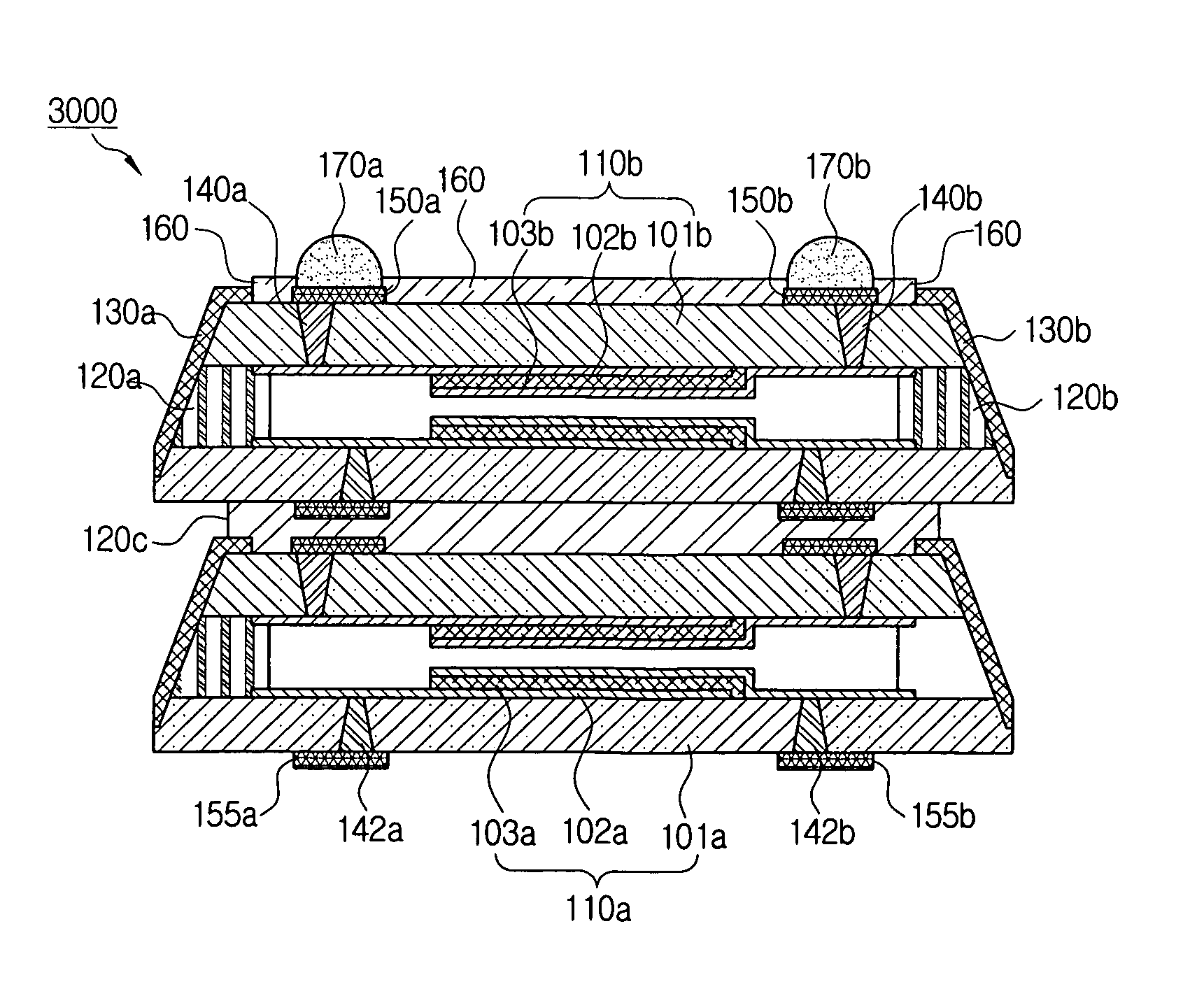
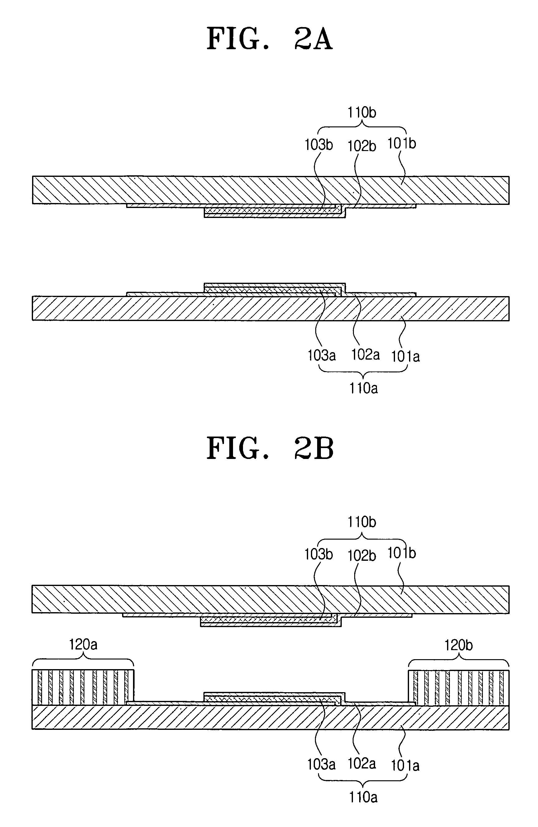
[0041]Hereinafter, exemplary embodiments of the present invention will be described with reference to accompanying drawings. Further, like elements are denoted by like reference numerals throughout the disclosure.

[0042]As well known, if a semiconductor wafer is manufactured through usual wafer manufacturing processes, individual chips are separated from the wafer and goes through packaging processes. The packaging processes are completely different processes requiring different facilities and raw material from the wafer manufacturing processes. However, exemplary embodiments of the present invention can enable manufacture of a package as a complete product even in a state that the individual chips are not separated from the wafer. Further, exemplary embodiments of the present invention can enable even use of the existing wafer manufacturing facilities and processes for the packaging facilities and processes, which indicates that the additional raw material for packaging can be minim...


PUM


Abstract

A micro package, a multi-stack micro package, and a manufacture method therefor are provided. A micro package according to the present invention includes a device substrate for mounting a devices, being a circuit module; a protection cap for protecting the device; bonding substances which, formed by patterning on predetermined areas on the device substrate, bond the device substrate and the protection cap; layers formed on a portion of the device substrate and a portion of the protection cap and exterior sides of the bonding substances; vias which are formed by etching away another portion of the protection cap, and electrically connected to an upper surface of the device substrate through the bonding substances; under barrier metals (UBMs) formed on the vias; and solder bumpers, being connection terminals for an external signal, formed on the UBMs. As stated above, the present invention has advantages of guaranteeing the hermetical sealing since the above layers prevent moisture absorption from outside at the same time of lowering possibility of damages to the device inside the package since the processing temperature drops below 150° upon wafer bonding due to the use of the polymer substance as a bonding substance.

Description

CROSS-REFERENCE TO RELATED APPLICATIONS[0001]This application claims priority under 35 U.S.C. § 119 from Korean Patent Application No. 10-2005-0064314, filed on Jul. 15, 2005, the entire contents of which are incorporated herein by reference.BACKGROUND OF THE INVENTION[0002]1. Field of the Invention[0003]Apparatuses and methods consistent with the present invention relate to a micro package, a multi-stack micro package and a manufacturing method therefor, and more particularly to a micro package, a multi-stack micro package and a manufacturing method therefor capable of guaranteeing hermitical sealing of a package and preventing damages to inside devices of the package.[0004]2. Description of the Related Art[0005]A today's trend in electronics industries is to manufacture light-weighted, compact, high-speed, multi-function, and high-performance products at low cost together with high reliability. The package assembly technologies are one kind of important technologies enabling the d...

Claims


Application Information

Patent Timeline
Patent Type & Authority Patents(United States)
IPC IPC(8): H01L23/34H01L23/48H01L23/52H01L29/40
CPCH01L24/11H01L24/16H01L24/94H01L24/97H01L25/0657H01L25/105B81C1/00269H01L23/053H01L23/055H01L23/10H01L23/147H01L23/49816H01L23/564H01L2924/00011H01L2224/293H01L2224/2929H01L2224/0401H01L2224/0557H01L2225/1035H01L2924/0002H01L24/83H01L2224/11831H01L2224/13025H01L2224/13099H01L2224/16H01L2224/2518H01L2224/274H01L2224/48463H01L2224/83851H01L2225/06524H01L2225/06527H01L2225/06541H01L2225/06551H01L2225/06586H01L2924/01013H01L2924/01022H01L2924/01029H01L2924/0103H01L2924/01047H01L2924/01049H01L2924/01078H01L2924/01079H01L2924/01082H01L2924/14H01L2924/1433H01L2924/30105H01L24/02H01L24/48H01L2224/9202H01L2924/01005H01L2924/01006H01L2924/01023H01L2924/01024H01L2924/01033H01L2924/014H01L2224/29075H01L2924/00014H01L2224/05552H01L2224/04042H01L24/05H01L2224/023H01L2224/45099H01L2224/45015H01L2924/207H01L2924/0001H01L23/12
Inventor KWON, JONG-OHKIM, WOON-BAESONG, IN-SANGLIM, JI-HYUKHAM, SUK-JINJEONG, BYUNG-GIL
Owner SAMSUNG ELECTRONICS CO LTD
Why Eureka
Try Eureka