Light-emitting semiconductor device

a technology of semiconductor devices and light-emitting semiconductors, applied in the direction of semiconductor/solid-state device manufacturing, semiconductor devices, electrical equipment, etc., can solve the problem that the gallium nitride-based compound semiconductor layer can barely obtain ohmic characteristics, and achieve the effect of preventing driving voltage from increasing, preventing the transparency of transparent conductive films and preventing the reflection of films from decreasing

Active Publication Date: 2007-11-06
TOYODA GOSEI CO LTD
View PDF10 Cites 63 Cited by
  • Summary
  • Abstract
  • Description
  • Claims
  • Application Information

AI Technical Summary

Benefits of technology

[0051]Effects to be obtained by the present invention are explained as follows.
[0052]The insulation protection film suppresses interface reaction of the reflection film and the transparent conductive film. As a result, a driving voltage can be prevented from increasing. When the first electrode layer is a transparent conductive film, both transparency of the transparent conductive film and reflectivity of the reflection film can be prevented from decreasing. Then luminous output efficiency of lights outputted through the light-transmitting substrate can be improved.
[0053]When electricity is conducted, electric current flows into the transparent conductive film only from the contact part of the electrode layer and the transparent conductive film owing to the insulation protection film. That enables to remarkably decrease possibility of generating electromigration of the reflection film. When the entire surface of the reflection film is covered by the insulation protection film, electromigration of the reflection film can be prevented from generating more certainly.
[0054]In the present invention, the materials of the first electrode layer can be different from that of the reflection film. So the metal used to form the first electrode layer can be replaced with a material which has excellent ohmic contact to the contact layer, and that enables to reduce driving voltage of the light-emitting device.
[0055]According to another aspect of the present invention, the first electrode layer is formed to expose a portion of the contact layer. That enables to pass light emitted from the active layer through the exposed portion of the contact layer, reflect the light effectively by the reflection film having high reflectivity, return the light to the semiconductor layer, and finally radiate to the outside of the device through the light-transmitting substrate. Further, this electrode has structure in which the light-transmitting insulation protection film prevents the reflection film having high reflectivity from contacting electrically to the first electrode layer and to the contact layer. As a result, driving voltage increase owing to alloying of metal atoms comprised in the reflection film and metal atoms comprised in the first electrode layer may not occur, and the interface between the semiconductor and the first electrode layer doest not change. Accordingly, materials and structure of the electrode is comprehensively excellent in electricity, optics, and reliability.

Problems solved by technology

Generally, because of a Schottky barrier existing at the interface between the compound semiconductor and the metal, the compound semiconductor comprising a gallium nitride based compound semiconductor layer can hardly obtain ohmic characteristic only by depositing a metal electrode on a semiconductor layer.

Method used


Image

  • Light-emitting semiconductor device
  • Light-emitting semiconductor device
  • Light-emitting semiconductor device

Examples


embodiment 1

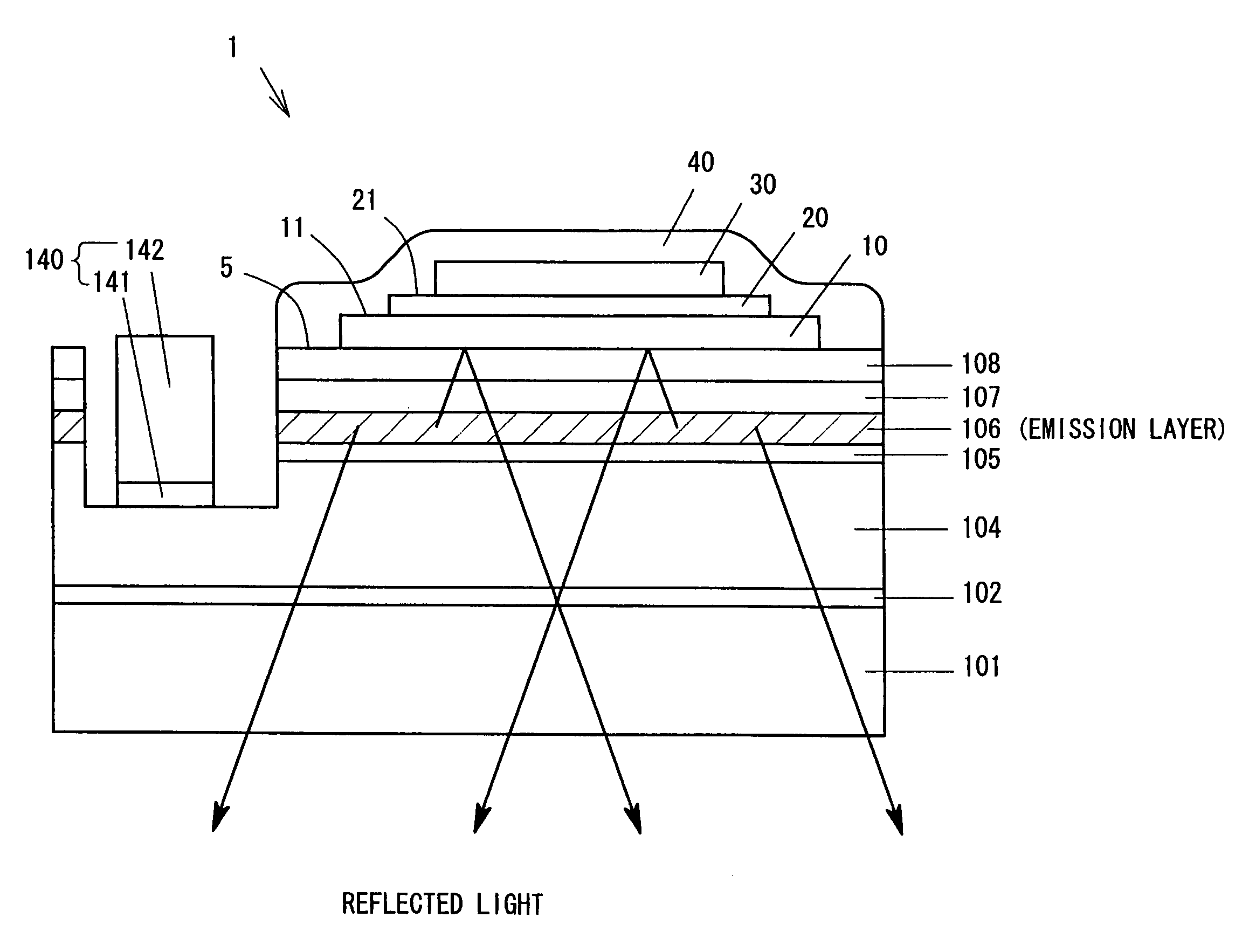
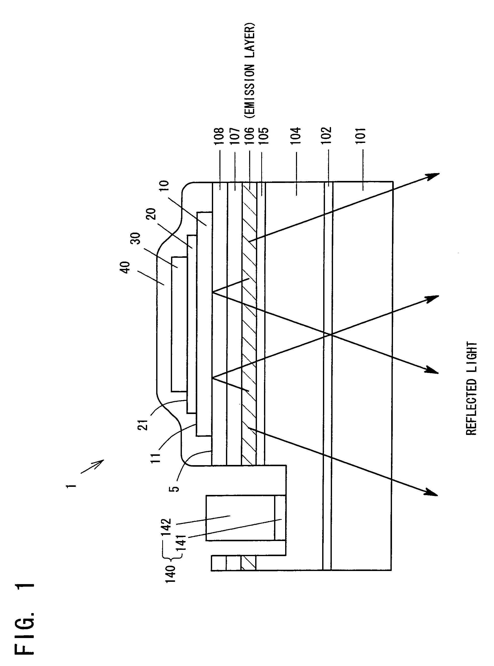
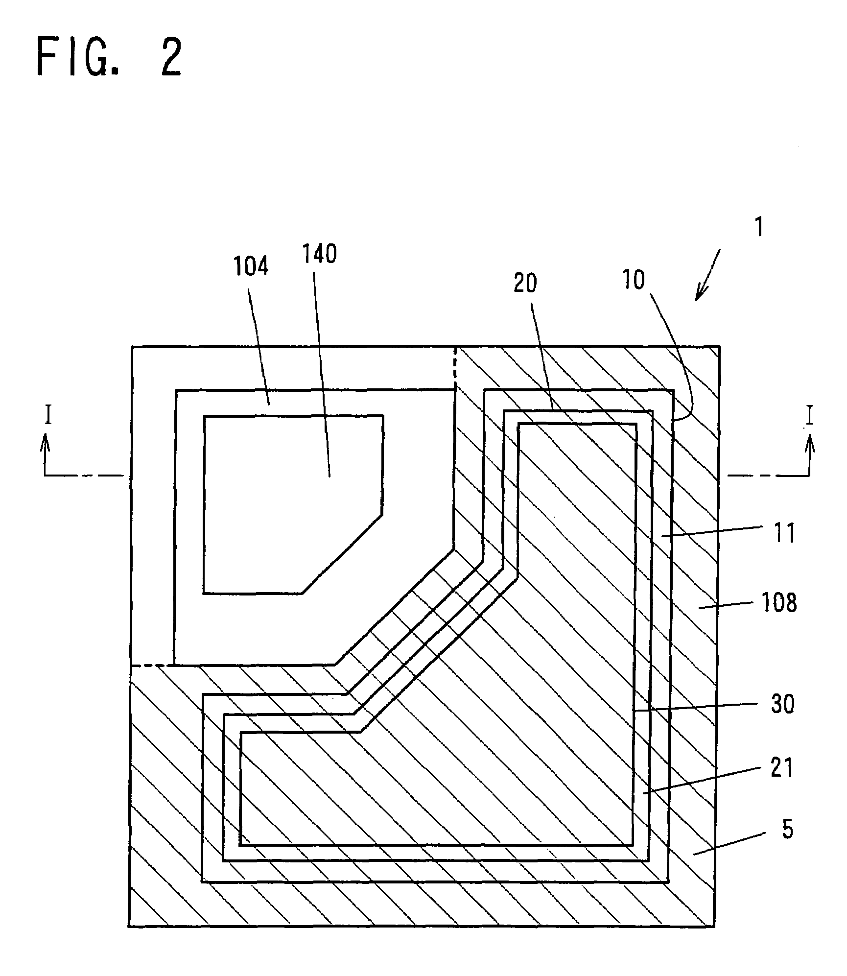
[0089]FIG. 1 is a sectional view and FIG. 2 is a plane view of a light-emitting semiconductor device 1 in the present embodiment 1. About 20 nm in thickness of aluminum nitride (AlN) buffer layer 102 is formed on 100 μm in thickness of light-transmitting sapphire substrate 101. About 8.0 μm in thickness of silicon (Si) doped GaN high-carrier concentration n+-layer is formed thereon as an n-type contact layer 104. The n-type contact layer 104 has electron concentration of 5×10¹⁸ / cm3. The higher the electric concentration of the n-type contact layer 104 is, the more preferable, and it is possible to increase the electric concentration to 2×10¹⁹ / cm3. And 200 nm in thickness of In0.03Ga0.97N strain relaxation layer 105 is formed on the n-type contact layer 104. An emission layer 106 having multiple quantum-well (MQW) structure which comprises 3 periods in total of about 20 nm in thickness of undoped GaN and about 3 nm in thickness of undoped Ga0.8In0.2N is formed on the strain relaxatio...

embodiment 2

[0096]A light-emitting semiconductor device shown in FIGS. 3, 4, and 5 is manufactured as explained in the best mode for carrying out the present invention, respectively. The light-emitting semiconductor device has effect similar to the device manufactured in the first embodiment. Each member which is shown in FIGS. 3, 4, and 5 and has same number as members in FIGS. 1 and 2 corresponds to each component in the first embodiment and in the best mode for carrying out the present invention.

[0097]FIG. 3 illustrates a device which does not comprise the first exposed portion and the third exposed portion but comprises only the second exposed portion 11 in L-shape at the right side A and the bottom side B. The transparent conductive film 10 made of ITO is formed in the same plane form as the p-type contact layer 108, and the insulation protection film 20 made of SiO2 is formed in the same plane form as the reflection film 30 made of Ag. And the electrode layer 40 made of Au is formed to co...

embodiment 3

[0099]Next, Embodiment 3 of the present invention is explained as follows.

[0100](Crystal Growth of a Gallium Nitride Compound semiconductor)

[0101]As a substrate to grow a gallium nitride based compound semiconductor thereon, a sapphire substrate 310 is used. After carrying out washing and vapor phase etching treatment, about 20 nm in thickness of AlN low temperature deposition buffer layer 311, about 4 μm in thickness of Si-doped GaN n-type layer 312, an active layer 313 which has multiple quantum-well (MQW) structure and is made of GaN and GaInN, 60 nm in thickness of Mg-doped AlGaN p-type layer 314, and 150 nm in thickness of Mg-doped GaN p-type layer 315 are deposited on the sapphire substrate 310 in sequence through metal organic vapor phase epitaxy (MOVPE) (FIG. 6). Alternatively, in order to obtain 280 nm of luminous wavelength, a Si-doped AlGaN layer is used as the n-type layer 312 and the active layer 313 having multiple quantum-well (MQW) structure is formed by using AlGaIn...


PUM

PropertyMeasurementUnit
reflectivityaaaaaaaaaa
widthaaaaaaaaaa
thicknessaaaaaaaaaa

Abstract

A flip-chip type of Group III nitride based compound semiconductor light-emitting device comprises a transparent conductive film 10 made of ITO on a p-type contact layer. On the transparent conductive film, an insulation protection film 20, a reflection film 30 which is made of silver (Ag) and aluminum (Al) and reflects light to a sapphire substrate side, and a metal layer 40 made of gold (Au) are deposited in sequence. Because the insulation protection film 20 exists between the transparent conductive film 10 and the reflection film 30, metal atoms comprised in the reflection film 30 can be prevented from diffusing in the transparent conductive film 10. That enables the transparent conductive film 10 to maintain high transmissivity. As a result, a light-emitting device having high external quantum efficienty can be provided.

Description

[0001]This is a patent application based on Japanese patent applications No. 2004-288880 and 2004-284075 which were filed on Sep. 30, 2004, and Sep. 29, 2004, respectively, and which are incorporated herein by reference.TECHNICAL FIELD [0002]The present invention relates to a light-emitting semiconductor device. Especially, the present invention relates to a flip-chip type light-emitting device which radiates lights from a transparent substrate side, having improved external quantum efficiency and suppressed age-related deterioration.[0003]Especially, the present invention relates to a light-emitting semiconductor device comprising a gallium nitride based compound semiconductor. Especially, the present invention relates to materials and structure of an electrode having electrically and optically excellent reliability about a flip-chip type of a light-emitting semiconductor device.BACKGROUND ART[0004]Progress in a light-emitting semiconductor device is remarkable in these days. Espec...

Claims


Application Information

Patent Timeline
Patent Type & Authority Patents(United States)
IPC IPC(8): H01L29/22H01L27/15H01L33/32H01L33/40H01L33/42
CPCH01L33/405H01L33/32H01L33/42
Inventor KOJIMA, MASANORIHIROSE, MINORUKAMIYA, MASAOYAHATA, KOSUKE
Owner TOYODA GOSEI CO LTD
Why Eureka
Try Eureka